|
Simplified method of design: estimation of performance.
An electronic voltage regulator is a most useful device, particularly for test gear and such apparatus where mains voltage fluctuations are troublesome. Many types are known, but it is proposed in this article to concentrate on one particular circuit and some modifications to it; to show how a suitable regulator can be designed in a simple manner. The circuit is the one which I consider to be most universally applicable to radio work.
Much has been published on the subject, particularly in the literature of physics, but with few exceptions these articles describe particular stabilisers and give details of their performances, good, bad and indifferent, which is of little help to busy engineers. The formulae which have been published are, in general, inapplicable without considerable information on the valves to be used, in such a way that direct measurements are usually necessary. Other writers emphasise the methods of designing the power unit, and gloss over the actual electronic stabiliser. I may have been unfortunate, but the many articles I have read in the past years on the subject all fall to a greater or lesser extent under these strictures. The reason is not far to seek, to my mind. It is that in practice there is no alternative to 'hit and miss', and a good deal of intelligent guessing. I am therefore describing in detail the method of controlling the guesswork which I have evolved for my own use, which has served well for some years, and has helped to design regulators which are not based on unsound operating conditions. The method is empirical, and can usually be completed on paper from makers catalogues and figures with a reasonable hope of obtaining the desired results.
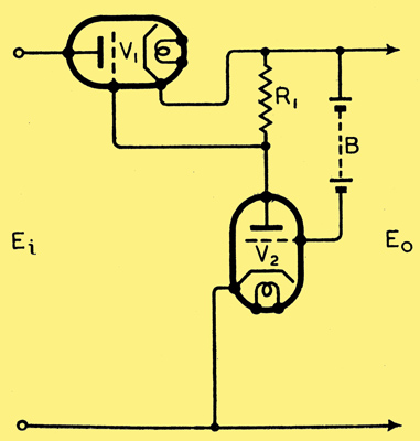
Fig. 1. Basic circuit of type of voltage regulator discussed in this article.
The basic circuit is shown in Fig. 1. The input from a rectifier or other source is passed to the load through a valve V1. This valve obtains its bias from the anode current of V2 through R1. The anode current of V2 is controlled by the battery B. It is clear that if the input voltage rises, the output voltage tends to rise. This causes the grid of V2 to become more positive, which increases the anode current through R1. This biases V1 more negatively, and hence reduces the variation of output voltage by an amount depending on the amplification of the circuit V2 R1, and the slope of V1, among other things. Obviously the battery B has to be of slightly higher voltage than the required output, which is very inconvenient, although other more economical arrangements are possible.
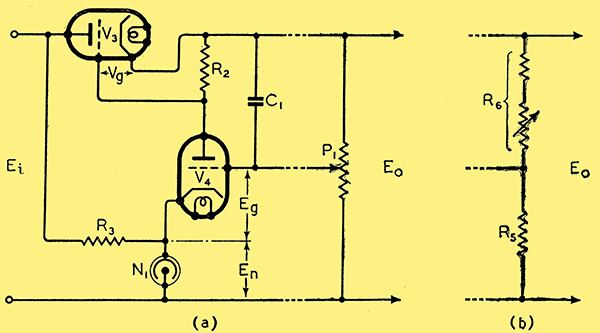
Fig. 2. (a) Circuit arrangement using a neon lamp instead of the battery in Fig. 1. (b) Practical arrangement of potentiometer P1.
For all normal purposes we can, fortunately, use a gas-filled stabiliser tube instead of the battery B, by rearranging the circuit as shown in Fig. 2 (a). N1 holds the cathode of V4 at a definite voltage above earth. P1 is adjusted so that the voltage on the grid of V4 is the required amount below the voltage on its cathode.
Some users of these circuits complain that they require adjustment very frequently, and that they are not inherently very stable, unless batteries are used in place of the gas discharge tube. In using such device I have found a good many unstable and variable ones, but the trouble has always been due either to amplifier instability, i.e. tendency to oscillate, or to the potentiometer P1. This latter is often made high, from 100 kΩ to 2 MΩ. Now the grid of V4 is not supposed to take current, neglecting leakage, etc. What happens is that, although the total resistance of P1 remains constant, the tapping point appears to vary from time to time, usually taking up a different value each time the apparatus is switched on. This is not surprising, considering the absence of current through the tapping point; and when the voltage across the resistance is of the order of maybe a hundred Volts or more, it is obvious that a minute variation in resistance will produce a noticeable variation in bias on V4. It is interesting to work out the degree of constancy required for P1 for a given case . After that, the maker of the potentiometer will no longer be blamed! A better device than the potentiometer is a combination of fixed and variable resistances, as shown in.Fig. 2 (b). In any case, the variable resistance should be wire-wound.
The design may now be started. Let us assume some values for an example:-
- Output voltage Eo to vary from 350 to 190 Volts, continuously.
- Output current Io to vary from 75 to 10 mA, independently.
- Mains input to rectifier varies ±8%.
- Regulation of rectifier from 10 to 75 mA, 10%.
- Stabiliser tube working voltage 55. (STC type 4313C.)
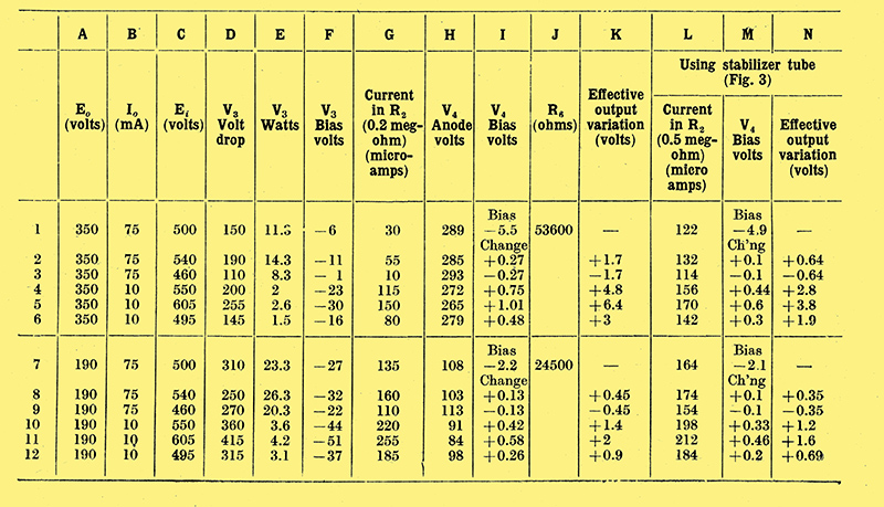
The next step is to make a table. Columns are lettered and rows numbered so that any square may be identified. Columns A and B are filled in thus: Rows 1, 2 and 3 are filled in with Eo max and Io max in each case. Rows 4, 5 and 6 have Eo max lo min. Rows 7, 8 and 9 have Eo min Io max, and finally the remaining rows Eo min Io min. Each row in the four sets is for normal, maximum and minimum rectifier output voltages (Ei, column C). Assume a safe value of 150 Volts for the drop across V3 in row 1 column D. Obviously C1 is then 500 Volts. C2 and C3 are therefore plus and minus 8% on this figure. C7, C8 and C9; correspond to C1, C2. and C3; the remaining rows have a further 10% added for the rise due to the regulation, as the current is low. We can now fill in the rest of D, Ei - Eo, whence column E Watts dissipation in V3. Having completed the table thus far, we must find a suitable valve for V3. A D024 or PX25 triode suits excellently. But, as we know the anode current and voltage of this valve, we can read off the necessary bias from the maker's anode current/anode voltage curves, which gives column F.
R2 must now be chosen. In general it will not be found advantageous to use a higher value than 0.1 or 0.2 MΩ. Although the stage gain rises as R2 is increased we have a fixed Volt drop across R2. The decrease in anode current which follows means reduced slope in the valve, so, that a compromise must be made.. In this example 0.2 MΩ will be assumed. The voltage across R2 is given in F, so that we can at once complete G, the current through R2. We must now choose V4. Let us take a 6Q7G, a high-mu triode. Column H shows the voltage across this valve, found by subtracting from A the stabiliser tube drop, 55 Volts, plus F. From the maker's curves we can then get the corresponding bias for the given anode voltage end current in V4, which we fill in I. As high values of R2 are used, however, it may be difficult to read the curves closely enough, To get over this difficulty we fill in 1.1 and 1.7, and then enter in the rest of I the changes in bias which have to be made.
The maker's- anode current/ anode voltage curve helps us here. The amplification factor of the valve is near enough a constant. By means of this fact, and a little careful interpolation, all the necessary information can be obtained. If we read off the corresponding anode voltages at the required current for two adjacent bias curves we can interpolate to find the bias corresponding to the known anode voltage.
The Potential Divider
The next. step is to evaluate R6 and R5 in Fig. 2 (b), which replace P1. A convenient value for R5 would be 10 kΩ. This will result in a constant bleed current of about 5 mA. The relationship between the resistances is:-
R6/R5 = | (Eo - En + Eg)/(En - Eg) |
|
As Eg is so small we may approximate:-
We then get two extreme values for R6 corresponding to the maximum and minimum values of Eo = 53,600 and 24,500 Ω. It is worth while to split R6 into a fixed portion and a variable, so that it cannot be reduced below 24,500 Ω. These values should be built up on test, so that the correct operating range is covered and no more, otherwise the regulator may be unjustifiably blamed for failure. In this case a variable of 50,000 Ω would be suitable. On test the value of 24,500 Ω should be built up until the lowest allowable output is attainable on minimum current and maximum mains volts, the variable being at minimum. The variable can then be shunted by a fixed resistance of the order of 75,000 Ω, so that at maximum variable resistance the maximum voltage and current output are obtained on low mains volts.
This adjustment takes about as long to do as to describe, and is a good safeguard in exchange for a couple of extra fixed resistances. In what follows, the built-up values of R6 are treated as single resistances.
The potential divider formed by R5 and R6 reduces the efficiency of the regulator by a factor:-
Remembering this, the performance of the whole may be tabulated in column K. K.1 and K.7 are reference points, the others are found thus: K.2. is given by: (R5 + R6)/R5 times the bias difference I.2, and so on.
This is the actual change of output voltage, which we have saved ourselves much difficulty by assuming absent. Fortunately, this is quite near enough for practical purposes. We have now completed the design of the circuit shown in Fig. 2 p(a) and (b).
A glance at the table shows that there are three lines only which are of major importance. These are:-
- Line 3, when Ei is a minimum, and Eo and I are both at maximum. In this case the bias on V3 is a minimum, and must obviously be kept to -1 Volt or even more.
- Line 8, when Ei and Io are maximum, and Eo minimum. This gives maximum watts dissipation on the anode of V3. If valve manufacturers did not read Wireless World, I would admit that I usually allow a 10% margin over maker's rating, as the condition is not often a working one.
- Line 11, when Ei is a maximum and Eo and Io are both at minimum. In this case the anode voltage on V4 is at its lowest, and the corresponding anode current is at maximum. The limit is the lowest desirable bias on V4, which may be -0.75 Volt.
If we are sure that V3 and V4 are being arranged to work efficiently, and are going to have the right order of voltages on them, these three lines are all that need be worked out for a new design, but until all pitfalls are understood, it is better to work out the complete table, and to study the effect of the various obvious changes of values which would be made.
This worked example is a very inefficient regulator, but it has been deliberately chosen so that the principles of operation may be clearly understood. A considerable improvement would be obtained by using say a Brimar 8D2 pentode in place of the 6Q7G, as is mentioned later. In more efficient regulators, the bias changes often become so small as to be difficult to estimate, and the experienced designer will merely ensure that V4 works at the maximum efficiency allowed by conditions, using the table only for V3. When the necessary test gear is available, the overall amplification of this stage V4 may be measured at audio frequency under the various working conditions, and the optimum values then chosen for a particular case. This is especially useful in the case of the screen voltage on a pentode, which sometimes prefers rather peculiar values.
Now even if we use the best possible arrangement of this circuit there is still a residual change, small though it may be. Let us consider how this can be improved. Obviously V4 cannot work under the best conditions, as typified by ordinary resistance-coupled amplifier technique, with a given anode resistance, because of the limited anode voltage across the resistance, with correspondingly low anode current. The circuit of Fig. 3 shows a method of dealing with this. If we use the same anode resistance as before, the anode current will be increased greatly, or alternatively, the anode resistance may be raised for the same current.
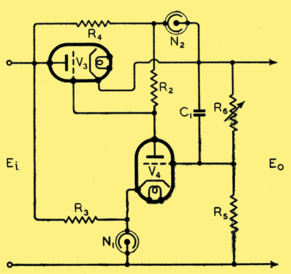
Fig. 3. Circuit designed to increase the efficiency of V4.
Two components only are added, R4 and N2. R4 is chosen to bring the tube current to a reasonable value. If a 4313C stabiliser tube is used, it might be about 50 kΩ in our example. The voltage in D shows the range that the tube has to cover without exceeding the maximum current rating. The maximum current is about 7 mA, s0 that this requirement is met. At the other extreme the minimum current will be of the order of 1 mA - this is also in the regulating range of the tube. Now it is clear that the change to the circuit has increased the volt drop across R2 by the amount of the tube drop, 55 Volts. We can now fill in columns L, M and N of our table. We take advantage of the increased voltage to raise R2 to 500 kΩ. Then by comparing K and N we can see the improvement obtained by using this device. Note that the voltage across V4 is unaltered. To be accurate, the currents in V3 should be recalculated, allowing for the shunt circuit across it. This shows the efficiency to be less, particularly at low currents, than appears from N.
It is seen that despite the apparent advantages at first sight of this method, which has been suggested by more than one writer, the actual improvement is slight, being greatest at the high-voltage, high-current end. In this case it is scarcely worth while to use the extra tube, but when the bias on V3 has a small range, close to zero bias, the method is valuable.
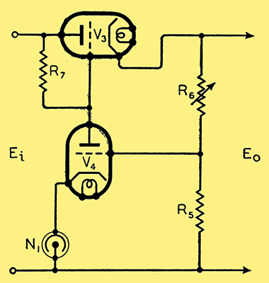
Fig. 4. Commonly used alternative circuit to that of Fig. 3 which is less efficient in practice.
A method often proposed instead of the above, with the same end in view, is simply to connect R2 to the anode of V3 instead of to the cathode, Fig. 4. Unfortunately this circuit is not as good as it looks. As the bias on V3 varies, so does the volt drop across V3. This volt drop across R7 varies in the same way, and in such a direction that it opposes regulation, i.e. it necessitates a correspondingly larger change in bias on V4. The increase in amplification obtained by the higher possible value of R7 and the higher anode current to V4 is usually much more than offset by the opposing variations. In fact it can be shown that if the amplification of V4 is constant in the two cases, the stabilising effect is reduced by a factor equal approximately to the amplification factor of V3. If V4 gives lower amplification, this must be allowed for in a comparison, but I have not met a case yet in practice where the balance was not in favour of the cathode connection.
It is necessary to point out here a disadvantage of the method of Fig. 3. First, stabilising tubes are not perfect, they have small spasmodic variations which may be of the order of a few tenths of a Volt. Each additional tube therefore has its deleterious effect. Secondly, the changes in current in column L are much smaller than in G. Thus any valve or circuit irregularities will show up far more in the former case. It is always as well to keep the anode current reasonably large, to minimise these spasmodic valve irregularities. Failure to do so has sometimes caused complaints of unstable regulation.
Supposing we want still better regulation. There are two little known devices we can use to improve matters. These were both described by Lindenhovius and Rinia in Philips Technical Review, Vol. 6, No. 2, 1941, which is not readily available in this country, and the principles involved will therefore be dealt with in detail. B Banerjee, in the Indian journal of Physics, Vol. 16, Pt. 2,1942, also puts forward similar ideas, independently.
There are two kinds of output variation we have to consider, variation caused by fluctuating input voltage, and that caused by fluctuating load. The methods to be described deal with these two cases.
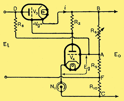
Fig. 5. Circuit with voltage and current compensation for fluctuations of input voltage and load.
Treating these points separately first, let us consider what must occur if the regulation were really perfect, as we assumed in our example. In Fig. 5 ignore for the moment R10. It is clear that for constant output voltage with varying input voltage, we would have to produce a certain change in voltage at A, across R6, related to the input variations. Now if we feed a small portion of the input voltage through R8 to A, the variation required will be obtained in the correct phase. In the table the first three lines show a change of input voltage of ±40 Volts. The corresponding change on the grid of V4 is approximately ±0.27 Volt. Then if R5 is 10 kΩ and R6 53,600 Ω, the required value of R8 will be about 1.25 MΩ. (R5 and R6 are effectively in parallel, as if the regulation is perfect, the internal resistance as seen across the output terminals is zero.) Of course a different value of R8 is required for each output voltage: for lines 7, 8 and 9 in the table it should be nearly 2.25 MΩ. In practice it is often possible to compromise; an intelligent guess is made at R8, which is made variable, and a good compromise found by experimentally varying the input voltage and noting changes. The compromise value is then built up from a number of fixed resistances as may be required.
Here again we have made an assumption which must not be overlooked. Obviously the current through R8 will increase the voltage drop across R5. To keep the output voltage constant in the first case above, R6 would have to be increased to about 57,500 Ω. In practice this can usually be neglected.
The second case may be considered similarly, ignoring R8 in Fig. 5. If the output voltage is constant, variations in load cause changes in the load current. This means that corresponding changes must be applied to point A as above. This can be done by adding R10 and thus changing the position of R5. R10 may be estimated as was R8. A variable resistance of 100 Ω is good for experiment, and a compromise can usually be found which meets requirements. For the two voltages quoted, the values of R10 would be 15 and 8 Ω approx.
If both voltage and current compensation are used together, as shown in Fig. 5, rather lower values of R10 are required, as owing to the impedance of the rectifier circuit, Ei, rises or falls as the current falls or rises. This reduces R10 above to 8 and 5 Ω. In other words, voltage compensation is a misnomer, for the first arrangement also gives a certain amount of current compensation.
These compensating devices usually render the stabiliser tube device of Fig. 3 unnecessary, except when a large power valve or valves are to be used over a range which is always close to zero bias.
When compromise is made in the values of the compensating resistances, perfect compensation is obtained only at one voltage or current, with over-compensation taking place on one side, and under-compensation on the other side. In practice, the approximately compensated circuit is almost invariably better at all points than the corresponding uncompensated one.
A further arrangement was suggested by Lindenhovius and Rinia which, they claim, enables the two compensations to be made independent of variation of output voltage caused by the controls. The method involves the setting up of a rather complicated bridge network, but might be of great value when the highest precision is required. Using this arrangement with battery bias instead of a stabiliser tube, an output variation of less than 0.004% is claimed for a mains variation of 5%. The circuit principle is shown in Fig. 6.
Fig. 6. Compensated bridge circuit suggested by Linden-hovius and Rinia.
The relationships of the network are given as:-
R11/R12 = | R15/R17 ≑ nμ - 1. |
|
and
R13/R12 = | R16/R17 ≑ nSR18 - 1. |
|
where
n = | overall amplification of V6. |
|
S = | mutual conductance of V5. |
|
μ = | amplification factor of V5. |
|
R14 is of suitable value to give the required output voltage variation. This circuit could obviously be adapted to use a stabiliser tube instead of a battery. I have not tried it, as all practical cases have so far been met with the other simpler circuits, but it is included for completeness, as it is not readily available elsewhere.
Practical Considerations
Turning now to practical points of design where experience is helpful, the following valves have been used very successfully:-
For currents up to 35 mA, 6V6G (triode connected). For currents up to 80 mA, D024 or PX25. For currents up to 120 mA, STC4300A. The control valve may be any type suitable for resistance-coupled amplification. Triodes have been shown above, but actually RF pentodes such as the 6J7G or Brimar 8D2 are very much better. The screen may be run from the output or input positive line through a dropping resistance or potentiometer; usually a very low voltage is best. If the screen voltage is obtained from the input voltage, some degree of compensation can be got by careful adjustment of the screen voltage. This method is not recommended, as in practice it is susceptible to variation. The series valve is not affected by the actual HT voltage level, but if high voltages are used, the control valve must be watched. Actually some standard RF pentodes have been reported as being used to control supplies of some thousands of Volts, but in these cases the valves must be chosen with great care.
In most radio applications it is advantageous for the stabiliser tube to operate at as low a voltage as possible. Here the STC 4313C is unique, as its volt drop is only 50-55 Volts at 1.0 to 10 mA. The Mullard 7475 is excellent when the higher voltage of 90 can be tolerated. The Cossor S130 has been used with success with a current as low as 9 mA through it, but this is not in accordance with makers ratings, as they recommend a very much higher tube current.
In constructing such a stabiliser it must be remembered that it is a high-gain amplifier, and must be made accordingly. For best results it is advisable to separate power pack and regulator, and not attempt to build them in one unit, because of the difficulty of eliminating hum pick-up on the amplifier. In no case when the amplifier has been properly designed and built has it been found desirable or necessary to use any extra devices to prevent instability. It is, however, always good to add a condenser C1 (Fig. 2). This may be 0.5 to 1 μF. It transfers direct, instead of through a potential divider, to the grid of the control valve all AF variations across the output. This usually improves the residual mains hum by large amounts, 25 dB or more, probably because the grid of the tube is tied down through a low impedance, and is therefore much less susceptible to pick-up.
As mentioned above, R6 should be wire-wound. It is best to insert in series with the variable the minimum calculated value so that the grid of V4 cannot be run positive into a region of poor or no control.
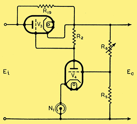
Fig. 7. By shunting V3 with a resistance a greater current output may be taken at the expense of some range of control.
There are no doubt many other dodges which will suggest themselves, but for reasons of space only one more will be mentioned which was proposed by Bosquet in Electronics, July 1938. Supposing we wish to take a large current from the stabiliser, the size of valve required may be excessive. By sacrificing range of control, however, we can pass a very much greater current through a given regulator by shunting the series valve with a resistance, R19 (Fig. 7). For instance, a regulator using one DO24 can be made to supply enough current for the heaters of a number of AC/DC valves in series. This can give much better regulation than a barretter or flux regulated transformer.
The shunt resistance must be adjusted rather accurately to the calculated value. The method of design is to add new columns B' and B'' to the table, for currents in resistance and valve respectively. Column D covers Watts in valve and resistance. If the valve to be used is known, B''8 gives the valve maximum wattage, so it can be filled in, whence B'8, and therefore R19. The rest of the table then follows. Clearly the shunt resistance limits both voltage and current range seriously. When only a fixed output voltage and current are required, as for valve heaters, etc., the table can be reduced to three lines only. Care must also be taken that the rectifier output is adjusted to the design value, as the limits for good regulation are rather close.
Valves can, of course, be run in parallel, but great care must be taken as if one valve takes an undue share of the current it may fail prematurely. Another valve then follows suit, and the first sign of trouble on one unit I was once shown did not occur until the third valve failed. This tends to be expensive. It is advisable to use valves in parallel much more conservatively and to choose types likely to match well. Grid stopping resistances may also be required to prevent parasitic oscillation. A method which may be useful to safeguard valves is to use a separate cathode resistance in each valve cathode lead, adjusting the values in such a way that any valve cannot take undue current. This involves the use of a separate winding on the heater transformer for each valve, unless indirectly heated valves are used.
In any case, it is particularly recommended that one transformer supply all the heaters, and that a separate one be used for the HT. The HT can then be switched on and off in the primary circuit. This saves quite a bit on capacitors and switching. If a wider range of voltage is required than is available in one range of control excess turns may be wound on the primary (with due regard to other considerations) to give reduced secondary voltage, or an auto transformer may be used. The number of ranges of control can thus be made as many as desired. It is better to control a wide range of voltage in steps, unless the current to be taken is very low. In the example, any greater voltage change would entail considerable reduction of the maximum current.
Heretofore the regulator has been considered only as a voltage stabilising device. It is, however, clear that it must have an internal resistance of low value. If stabilisation is perfect, the internal resistance (or more accurately impedance) must be zero. If there is overcompensation, the resistance is negative. This applies at all frequencies at which the control valve is an efficient amplifier.
This opens up a new field of use for the electronic regulator as an impedance which is sensibly zero to AC right down to the lowest frequencies, and yet has a DC potential across it. Regulators have been found invaluable, for example, in wide band amplifiers, for feeding screen circuits in such a way that compensation is not necessary at low frequencies. The device is also useful in coupling cathode ray tubes directly to amplifiers, as no auxiliary impedances are necessary. Moreover, regulators can be used to supply transmitter bias with advantage. The transmitter grid current would normally cause a considerable rise in grid voltage unless a heavy load is placed across the bias supply. If a regulator is used, it is only necessary that the load current be a little greater than the maximum grid current. Banerjee, in the paper mentioned before, proposes this idea in connection with the large Class B amplifiers, used in broadcast transmitters. It has also value in factory testing.
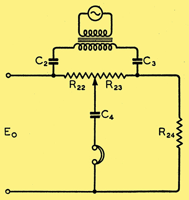
Fig. 8. Circuit for measuring the effective internal resistance of voltage regulators.
The use of regulators for such purposes does not yet seem to have had the attention it deserves; the applications mentioned are only indicative of the possibilities, being some I have found useful. In such applications, measurement of the actual internal resistance becomes interesting. The usual circuit is shown in Fig. 8. R22, R23 and R24 are together the required load on the regulator. An audio oscillator is fed through a transformer and two capacitors across R22 and R23, while the junction of these two resistances goes to the negative line via a capacitor and a pair of phones. If R22 and R23 are made from suitable variable and fixed resistances, the slider is adjusted for minimum sound in the phones. The internal resistance is given by:-
As an indication of the expected values, Ri for the sample regulator is of the order of 70 Ω maximum. Obviously this method can be adapted to use existing parts in a number of ways. If a cathode ray oscillograph is available, there are other useful methods. If Eo is applied to the CRO through a blocking condenser and amplifier, any residual mains hum will be seen. This can be used as a method of adjusting the voltage compensating resistance, provided the amplifier tube of the regulator does not pick up too much hum, which would mask the effect.
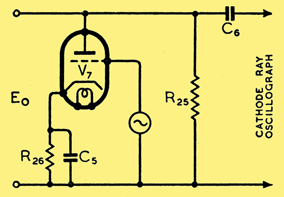
Fig. 9. Load circuit for use with CRO for visual adjustment of compensating circuits.
It is often necessary to know how the internal resistance (which is slightly inductively reactive) behaves when varying alternating voltages are applied across its output. This effect can easily be studied on the CRO in the following manner. The required load is made up of R25 and V7, Fig. 9. R26 biases V7 suitably as an amplifier. V7 is chosen so that by varying its grid potential its anode current is varied over a suitable range. To start with, an effective load variation of 5% might be aimed at. As the compensation is varied, so the amplitude of the CRO trace will be modified. An accurate compensation can be made at any frequency, or a frequency characteristic can be taken. Actual measurement can only be made indirectly thus, but it is nevertheless probably the most convenient practical method, provided great care is taken to see that the CRO does not pick up directly and so give spurious results.
The tube V7 could, of course, be placed across Ei, and thus voltage compensation adjustment made at a frequency other than that of the mains, if for some reason that is desirable.
Limitations of space prevent the fuller discussion of the many points which arise. This article is therefore only intended to indicate simple and useful methods which have been tried out over a number of years. The principles laid down, while not at all deep, enable a designer to estimate the performance of a regulator with little trouble, and with every expectation of getting the required answer without much experiment. No apology is therefore made for the elementary and unacademic approach to the problem.
The work described above was carried out by the writer during his employment with Messrs. Standard Telephones and Cables, Ltd., New Southgate, to whom acknowledgements are therefore due. Mr D N Corfield of the Sidcup Factory of that company, has also kindly helped by providing curves and figures for the 6Q7G valve.
Appendix
The appendix with the formula derivations can be found here.
|