|
Details of Chosen Circuit and Its Performance
May 1947
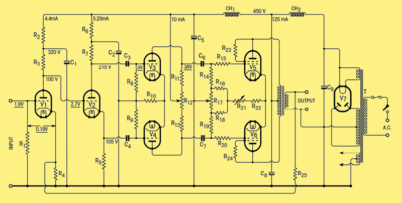
Fig. 5. Circuit diagram of complete amplifier. Voltages underlined are peak signal voltages at I5 watts output.
The considerations under-lying the design of a high-quality amplifier were discussed in the first part of this article. A circuit of the complete amplifier is shown in Fig. 5. This follows the basic arrangement of Fig. 3(b). The design of the individual stages will not be treated in detail, but a review of the salient features may be of value. As a measure of standardization all valves except those of the output stage are type L63, triodes of about 8,000 ohms AC resistance.
Initial Stages. In order to keep the phase shift in the amplifier at low frequencies as small as possible the first stage has been directly coupled to the phase splitter, eliminating one R-C coupling. The first two stages are thus designed as a single entity. The phase-splitter section, which consists of a triode with equal loads in anode and cathode circuits, operates partly as a cathode follower, its grid being some 100 V positive with respect to chassis. The anode of the first triode is also arranged to be about 100 V positive and is coupled to the phase-splitter grid. Due to the cathode-follower action of V2 the operating conditions are not critical and no trouble is likely to be encountered from normal changes in valve parameters. The cathode bias resistor of V1, to which feedback is applied from the output transformer secondary, is kept as small as practicable to avoid gain reduction in the first stage, due to series feedback.
Driver Stage. The output from the phase-splitter is taken to the push-pull driver stage. Provision is made for varying the load resistors of this stage which, in conjunction with a common un-bypassed cathode bias resistor, allows a considerable range of adjustment to be made in the drive voltages to the output valves to compensate for any inequality in gain.
Output Stage. The balance of quiescent anode current in the output stage is a matter of some importance, as it affects the performance of the output transformer to a marked degree. In this amplifier, provision is made, by means of a network in the cathode circuits of the KT66 valves, for altering the grid bias of each valve, giving complete control of the static conditions of the stage. A feature of this arrangement is that the valves operate with a common un-bypassed cathode bias resistor, which assists in preserving the balance of the stage under dynamic conditions.
Output Transformer. The turns ratio of the output transformer will be determined by the impedance of the loudspeaker load. It is convenient to make each secondary section of such an impedance that by series-parallel arrangement a number of suitable load impedances may be provided utilizing all the sections of the transformer. A suitable value of impedance is 1.7 Ω per section, giving alternatives of 1.7, 6.8, 15.3, 27 Ω, etc.
Winding data for a suitable transformer are given in the Appendix.
Negative Feedback Network. The design of this amplifier is such that no difficulty should be experienced in the application of negative feedback up to a maximum of some 30 db. Provided that the threshold of instability is not reached, the benefits of negative feedback increase as the amount of feedback is increased, at the sole expense of loss of gain, but there will be little if any audible improvement to be gained with this amplifier by increasing the amount of feedback beyond 20 db.
The feedback network is a purely resistive potential divider, the bottom limb of which is the cathode bias resistor of the first stage.
With component values as specified no trouble should be experienced from instability due to the effects of unintentional positive feedback. Should instability arise it will probably appear as oscillation at a supersonic frequency. This may be transient, occurring only at some part of the cycle when the amplifier is operated near maximum output. Its cause may be bad layout or an output transformer with a higher leakage reactance than specified, or it may be due to resonance in the output transformer.
A remedy, which should only be used as a temporary measure, is to reduce the high-frequency response of one of the amplifier stages, so reducing the loop gain at the frequency of oscillation to a value below unity. This may conveniently be done by connecting a small capacitor (say 200 pF) in series with a 5,000 Ω resistor from the anode of V1 to chassis.
PERFORMANCE
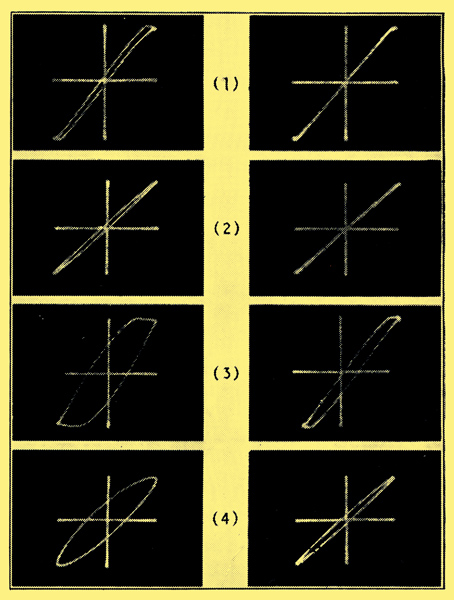
Oscillograms of input-output characteristic ; left-hand column, without feedback; right-hand column, with feedback. (1) At 300 Hz with slight overload (2) At 300 Hz, output voltage 15% below maximum. (3) and (4) Conditions as in (1) and (2) respectively, but at 30 Hz.
Linearity. The linearity of the amplifier is well illustrated by the series of oscillograms. These show that, up to maximum output, the linearity is of a high order, and that the overload characteristic is of the desirable type shown in Fig. 1(b) in the previous article. The improvement due to the application of negative feedback, especially at low frequencies, is clearly demonstrated by the oscillograms.
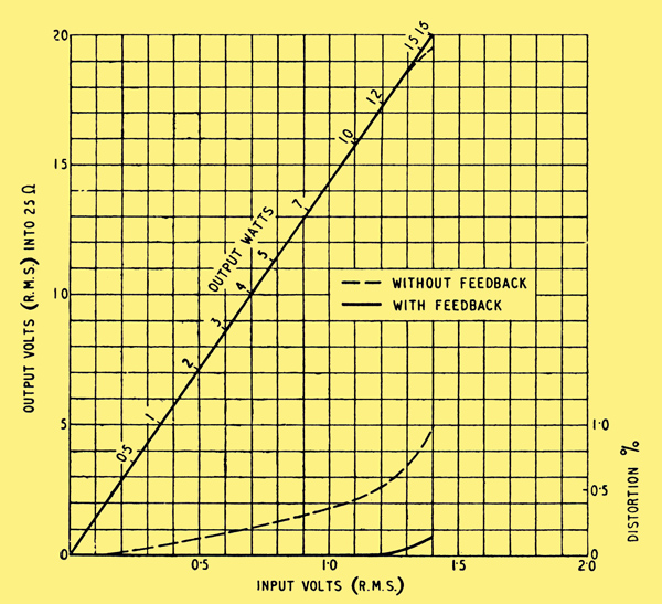
Fig. 6. Input-output characteristic and harmonic distortion curves, with and without feedback.
Equipment for measuring inter-modulation products was not available, but measurement of the total harmonic, distortion was made with an input frequency of 400 Hz. The result is shown in Fig. 6, from which it will be seen that the harmonic distortion at maximum rated output (15 Watts) is less than 0.1%. inter-modulation, with this degree of linearity, is not present to an audible degree.
Frequency Response.
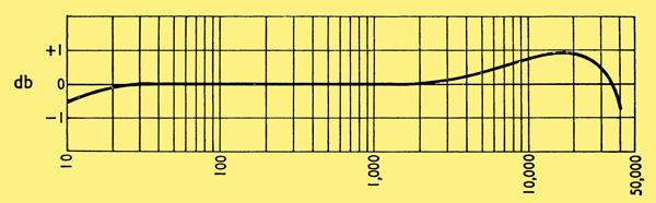
Fig. 7. Frequency response (without feedback) of 20 Watt output transformer described in appendix. Generator resistance 2,500 Ω load resistance I.7 Ω. Measured with 5 V RMS on primary. At higher excitations the bass response improves progressively up to saturation.
The frequency response of the amplifier is greatly dependent upon the characteristics of the output transformer. In the amplifier tested, the output transformer had a resonance at about 60 kHz which caused a sharp dip of 2.6 db around this frequency. The characteristic within the audible range from 10-20,000 Hz is linear within 0.2 dB.
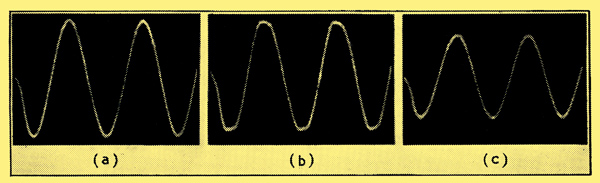
(a) Input waveform, 300 Hz. (b) Output waveform with feedback and slight overload. (c) Output waveform with feedback but output voltage 15% below maximum.
Phase Shift. The excellence of the frequency response characteristic indicates that little phase shift is present. Phase shift is only apparent at the extremes of the AF spectrum and never exceeds a few degrees.
Output Resistance. The out- put resistance of the amplifier is 0.5 Ω measured at the 15 Ω output terminals.
Noise Level. In the amplifier tested, the measured noise level was 85 db below maximum output. The noise in this amplifier was, however, almost entirely 50 Hz hum, caused by coupling between the mains and output transformers. By more careful arrangement of these components it appeared that the noise level could be reduced to better than 100 dB below maximum output.
If desired, the power output of the amplifier may be increased beyond 15 Watts by the use of several pairs of output valves in parallel push-pull. The output transformer, power supply and bias arrangements, and the feedback resistor R25 will require to be modified. Amplifiers of this design with power outputs up to 70 watts have been produced.
Listening tests carried out in conjunction with a wide-range loudspeaker system have fully supported the measured performance. No distortion can be detected, even when the amplifier is reproducing organ music including pedal notes of the 20 Hz order, which reach the threshold of maximum output. Transients are reproduced with extreme fidelity; tests using a direct microphone circuit with noises such as jingling keys reveal extraordinary realism.
The amplifier can be described as virtually perfect for sound-reproducing channels of the highest fidelity. It provides an ideal amplifier for sound-recording purposes, where 'distortionless' amplification and low noise level are of prime importance.
APPENDIX
Output Transformer. Specification.
- Primary load impedance = 10,000 ohms centre tapped.
- Secondary load impedance : 1.7 Ω per section. Turns ratio: 76 : 1.
- Primary inductance: 100 H (min.)
- Leakage inductance: 30 mH (max.)
Winding Data.
Core: 1.75 inch stack of Pattern No. 28A 'Super Silcor' laminations. (Magnetic and Electrical Alloys, Burnbank, Hamilton, Lanarks.) The winding consists of two identical interleaved coils, each 1.5 inch wide, wound on 1.25 in x 1.75 inch paxolin formers. On each former is wound: 5 primary sections each consisting of 5 layers (88 turns per layer) of 30 SWG enamelled copper wire interleaved with 2 mil. paper, alternating with 4 secondary sections, each consisting of 2 layers (29 turns per layer) of 19 SWG enamelled copper wire, interleaved with 2 mil. paper.
Each section is insulated from its neighbours by 3 layers of 5 mil. Empire tape. All connections are brought out on one side of the winding, but the primary sections may be connected in series when winding, only two primary connections per coil being brought out. Secondary connections for different ratios are given in the Table on page15.
Measured Performance.
Primary inductance: 100 H. (measured at 50 Hz with 5 V RMS on primary, equivalent to 2.5 mW) Leakage inductance = 22 mH. (measured at 1,000 Hz) Primary resistance = 250 Ω
Components
The valves specified are L63, KT66 & U52
|