|
Constructing the Triode Amplifier
There is a slight difference in the hook-up methods used with valve circuits compared with those using solid-state devices. The latter, because of their small size, lend themselves readily to strip-board construction. In contrast, the valve has to be plugged into a base, which is itself a relatively large component which must be physically attached to a panel with the necessary hardware. This is no great disadvantage, as in fact it provides a set of nine (in the case of B9A bases) useful wiring points. If a tag-strip is mounted nearby, then it is easy to hook up components between valve base pins and the tag-strip connections. To make life even easier, solder tags can be secured underneath the base mounting screws, so that ground connections can be made straight to the chassis.
An Experimental Chassis
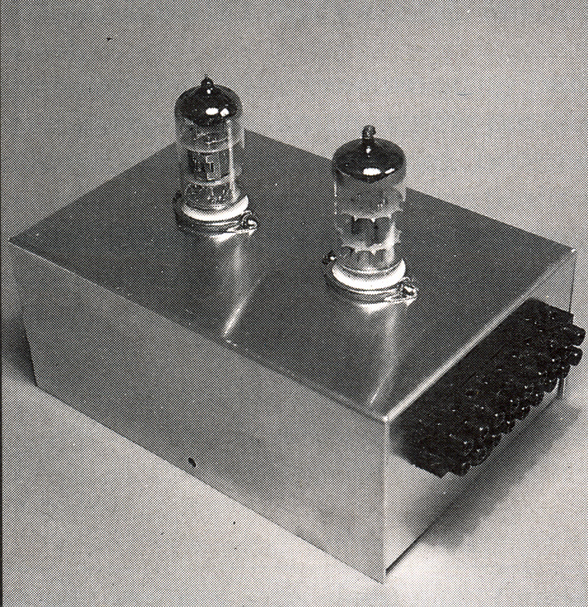
Completed chassis with valves in place.
While it is possible to build valve circuits on PCBs. it is more convenient (and more interesting) to use a more traditional aluminium chassis with round cut-outs in the top for chassis mounted valve bases. A tag strip can be mounted inside (or a tag board on pillars) to allow circuits to be hooked up and modified without too much aggravation. A suitable able chassis exists (Order Code XB56L) and the photographs show how this has been used for the purpose described. It is worth buying a ready made chassis like this as it saves the chore of bending raw sheet into shape, which is not easy to do neatly without specialised bending tools. The B9A bases (Order Code CR31J) used for the valves require a 22.5 mm (7/8 inch) diameter hole to be cut in the chassis, which is easily done using a 'Q-Max' hole punch (Order Code BA68Y). This also requires an 8 mm Allen key to turn it, but if this is lacking it is possible to use a suitably sized box spanner and tommy bar.
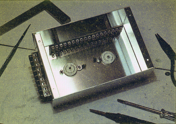
Underside view of experimental valve chassis, showing tag-strip for components and screw terminal block connector.
A tag strip on the inside of one long side allows for the mounting of components and as a 'jumping off point' for components or connections to the valve bases themselves. To take the power, both HT and LT, into the experimental chassis, a 'chocolate block' (screw terminal block) can be mounted at one end and the wiring run through to the interior of the chassis through a small hole, using a grommet for safety.
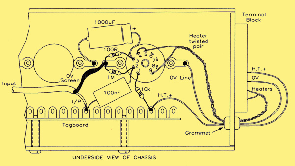
Component layout on experimental chassis for the triode amplifier design.
The diagram above shows the underside view of this chassis where the layout for the components used in this design can be: clearly seen.
It is usual when wiring up valve equipment to connect up the heater wiring first. This is always done in twisted pairs to reduce electromagnetic fields from the AC heater current. The terminal block at the end of the chassis can have a pair of terminals allocated for the heater connections, with a further twisted pair running from here back to the power supply. In the same way, a pair of terminals will also be allocated for the HT+ and 0 V connections, these running back to the power supply on suitably colour-coded wires. Although I used full wiring posts on my prototype power supply, the proper connectors to fit should be recessed 4 mm sockets, so make up 'proper' wire connections terminated in 4 mm plugs to connect at the power supply end, rather than simply using wires with bared ends!
The heater connections on the valve base are pins 4 and 5, with pin 9 as the centre-tap, but this orientation is for a 12.6 V heater supply: As explained in Currently Available Triode Valves, since we are using a 6.3 V supply, the two halves of the valve heater are connected in parallel. This is done by strapping pins 4 and 5 on the valve base together and running the heater twisted pair from the terminal block to the pins 4+5 and 9 respectively.
The HT connections were run so that one tag on the tag-strip was used for the +150 V supply, while the 0 V wire was taken directly to chassis by way of one of the solder tags, as shown.
The grid leak resistor R1 is hooked directly between pin 2 of the valve base and a solder tag. Similarly, the parallel cathode bias and decoupling components are taken straight from pin 3 to a solder tag. The input capacitor C1 is connected between the tag-strip and pin 2 of the valve. The anode load resistor R2 is similarly connected between pin 1 of the valve and the tag-strip. It actually takes only a few minutes to hook up a circuit of this sort. Not only that but it is easy to make changes, substitute other components, and so on, because the disconnections and reconnections are accepted as satisfactory and AC testing was then carried out.
Measurement of signal gain was carried out with an input of 1.7 V Pk-to-Pk (0.6 V RMS) at the test frequency of 1 kHz. The output voltage was measured as 30 V Pk-to-Pk (13 V RMS).
Thus, the mid-band voltage gain (VAF) = 13 / 0.6, = 21.67.
This compares extremely well with the design value for the VAF of 20. The output waveform was extremely clean with no discernible distortion.
This was true over the full band-width of the amplifier.
In order to measure the bandwidth, an analogue electronic voltmeter was used to set up an output reference of 0 dB at 1 kHz. Without any further adjustment of input signal level, the frequency was first reduced until the output fell by 3dB. the frequency at which this was noted was 6 Hz. The frequency was then increased until, at some high frequency, the output again fell by 3dB. The frequency on this occasion was 130 kHz.
The bandwidth of 6Hz to 130 kHz thus more than covers the audio-frequency range and in practice it would be necessary to make the high-frequency gain roll off at a rather lower frequency. However, that was not the object of the exercise on this occasion.
Effects of External Loads
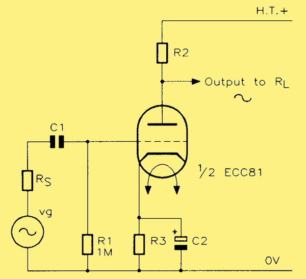
Basis for the design: circuit diagram for a single-stage triode voltage amplifier..
As shown above the amplifier is operating into an open circuit. While this may not be strictly realistic, it is not too far from what may be an actual operating condition. If the following stage was also a voltage amplifier of similar type, then its input impedance would be the resistance of its grid leak, at least up to the point where the input capacitance of the following stage started to be significant. Thus the 10 kΩ anode load would be looking into a 1 MΩ following impedance. This would have little shunting effect on the anode load and, hence, little effect on the voltage gain.
In any cases where the input impedance of the second stage was comparable to the value of the anode load of the first stage, then the effective load of the first stage becomes equal to these two impedances in parallel. In the equation for the VAF, these can be combined into a single equivalent term, Rl'.
Then:–
VAF = (μ x Rl') / (ra + Rl') - (Equation two a)
Alternative Expression for Voltage Gain
In Earlier in the series the VAF was stated as being given by the following expression:
VAF = gm x Req - (Equation Three)
This requires further explanation, especially in view of the fact that I have actually used a different expression for VAF (Equation two above) in the calculations for the gain of the amplifier – or have I? The truth is that the two equations are absolutely identical, merely two alternative ways of stating the same thing. This can be shown quite easily when we understand what Req means. It is, in fact, the parallel sum of ra and the anode load Rl. That is:–
Req = (ra x Rl) / (ra + Rl)
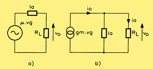
(a) constant voltage and (b) constant current equivalent circuits for a valve amplifier.
The diagram above shows two middle-frequency equivalent circuits for a valve amplifier. (a) is known as the 'constant voltage' circuit, while (b) is known as the 'constant current' circuit. The constant voltage circuit includes a voltage generator, whose value is μVg, feeding into ra and Rl in series. The voltage (Vo) across the load Rl is the output of the amplifier and, by proportion, will be as follows:
Vo = μVg x (Rl) / (ra + Rl)
If we divide both sides by Vg (the signal input), the left-hand side will be V0 / Vg, which is obviously the voltage gain, or VAF. What is left on the right-hand side once Vg has been removed will be recognised as the right-hand side of the original equation (Equation two). That should justify that equation; now for the constant current circuit.
The circuit of (b) may not look the same as that of (a) but it is directly equivalent to it. The voltage generator μVg feeding into a 'series' resistor combination has been replaced by a current generator gmVg feeding into a 'parallel' combination of the same two resistors. This time, instead of the output voltage dividing between two series resistors, the output current divides between two parallel resistors. The proportion of the total current that flows in Rl. produces the output voltage Vo by Ohm's Law. This current in Rl. is given by: gmVg(ra / (ra + Rl)), so that the output voltage will be as follows:–
Vo = gmVg x ((ra) / (ra + Rl)) x Rl
Again if we divide both sides by the input voltage Vg, the left-hand side will be equal to the VAF and the right-hand side will be equal to:–
(raRl) / (ra + Rl)
which is the parallel sum of these two resistance values, namely Req, as defined earlier.
What I have done here is to show that there are two different expressions for VAF, each taken from a different type of equivalent circuit. If you want to show that Equations two and three are equal, you can easily do so by using the relation that:–
μ = ra x gm
But i'll leave that up to you!
|