|
New high gain circuit.
The advantages of resistance-capacitance circuits for phase-splitting in push-pull amplifiers are now well recognized, a wide variety of circuits for this purpose having been evolved in the last decade or so. If these circuits are investigated it is found that they possess varying degrees of merit in producing symmetrical output voltages, but share the common disadvantage of inherently low gain. In fact, low gain would appear to be almost inherent in any phase-splitting arrangement. The circuit to be described in this article, however, will be shown to possess a very high degree of symmetry with, at the same time, a large amplification from only two valves. An overall amplification of more than 1,000 times can very easily be achieved with standard low-gm valves.
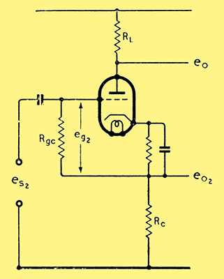
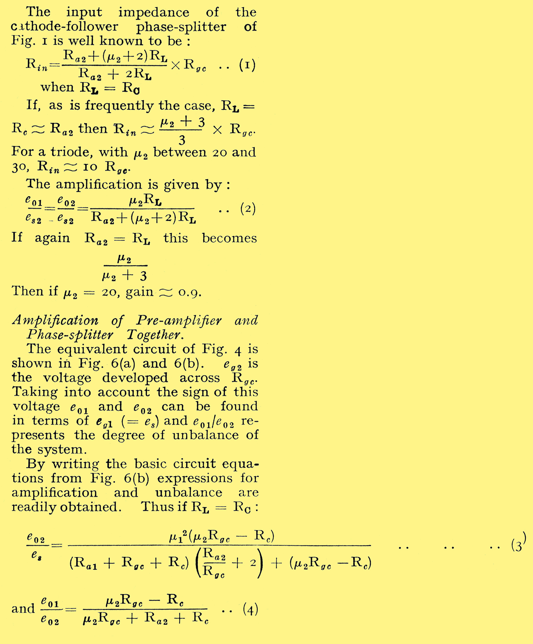
Fig. 1. The basic cathode-follower type of phase-splitter.
In order to facilitate analysis and to effect a just comparison with other types, the circuit will be compared with, and developed from, a normal cathode-follower phase-splitter preceded by a pentode AF stage.
For the purposes of this article the amplification of a phase-splitting system will be regarded as the ratio of either output voltage (assuming the two to be sensibly equal) to the signal input voltage (i.e., amplification = e01/es or e02/es in Fig. 2).
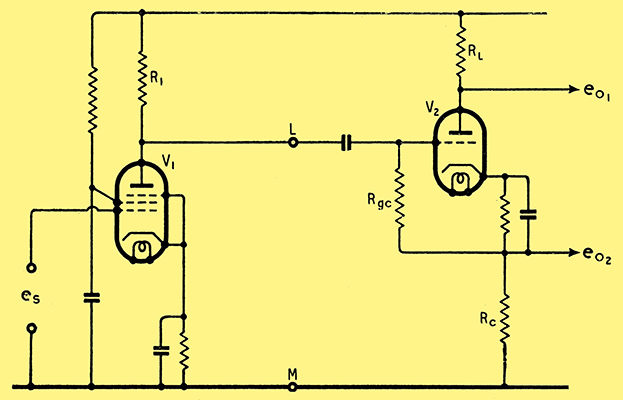
Fig. 2. The combination of a phase-splitter with a preceding AF stage is shown here.
In other words, the gain of the system as a whole is twice that given. The cathode follower, Fig. 1, is perhaps the most generally used circuit because of its simplicity and the high degree of balance obtainable between e01 and e02, at normal frequencies, being dependent, only on the accuracy of RL; and RC. It possesses, of course, the inherent disadvantage of a cathode follower in that its gain is slightly less than unity (Appendix Equation (2)).
If we now consider such an arrangement to be preceded by a pentode stage the circuit becomes that of Fig. 2 and the overall gain is nearly that of the pentode alone, about 100 times.
Let us now consider the factors which limit the gain of the circuit of Fig. 2. It is well-known that the input impedance of a cathode-follower is extremely high, approximately 10 × (impedance between grid and cathode); consequently if the grid-cathode impedance is made 250 kΩ the impedance to the right of 'LM' in Fig. 2 is 2.5 MΩ. In other words, the input circuit of V2 does not appreciably shunt R1 and the gain obtainable from V1 is determined almost entirely by R1. The value of this resistance cannot, however, be increased indefinitely, owing to the fall in steady anode voltage of V1 and a practical maximum is about 250 kΩ 500 kΩ. Since the AC resistance of the pentode is very high (say 2.5 M&Omega) it follows that only a small fraction of the amplification factor can be realized as gain (since gain = μR1/(Ra1 + R1). This is unfortunate, because the amplification factor is extremely high, about 4,500 being quite a normal value for a pentode.
Suppose, however, it were possible to use the very high input impedance of a cathode-follower as the actual load on V1. Then, since this impedance is comparable with the AC resistance of the pentode, the amplification obtained would be greatly increased.
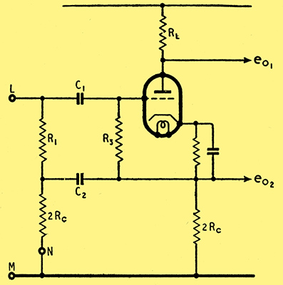
Fig. 3. A modified phase-splitter in which the coupling resistor R1 becomes part of the grid-cathode impedance of the cathode-follower.
If the circuit to the right of LM in Fig. 2 is rearranged as shown in Fig. 3, the parallel impedance of R1 and R3 replaces the grid-cathode impedance Rgc while the effective cathode load is still Rc. Consequently the AC conditions have not been changed by the rearrangement and the input impedance is still approximately 10 × Rgc (where Rgc = R1R3/(R1 + R3). It is assumed that the reactances of C1 and C2 are negligible at the lowest working frequency.
We cannot, as the circuit stands at present, connect the point L directly to the anode of V1 since there is no means of supplying anode current to V1. It will be seen, however, that N is at earth potential and there is no reason why we should not return this end of the resistor to + HT, which is also at earth potential, so far as AC is concerned. In this way we can provide a DC path to the anode of V1 without disturbing the AC conditions on V2, while V1 still sees the input impedance of V1, acting as a cathode follower, as its dynamic load.
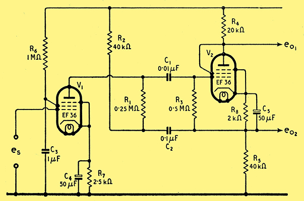
Fig. 4. The practical form of the high-gain phase-splitter and preceding stage.
The final phase-splitting circuit becomes that of Fig. 4, in which the component values are those used in the experimental model.
Using an EF36 strapped as a triode for V2, Ra2 = 10 kΩ and μ = 28; with the component values of Fig. 4 Equation (1) gives the input impedance Rin as 2.05 MΩ. It will be noted that R1R3/(R1 + R3) = 168 kΩ.
Then the amplification of V1 is given by μ1Rin/(Ra1 + R1 = 2030) where μ1 = 4,500 and Ra1 = 2.5 MΩ.
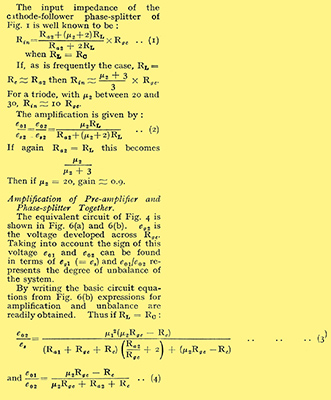
The gain of V2 as given by Equation (2) is 0.9; therefore the overall gain of the system e02/es = 2030 × 0.9 = 1860. It is of interest to note that Equation (3) in the Appendix, which was derived directly from the equivalent circuit of Fig. 6(b), gives the same value as that obtained by the foregoing physical argument.
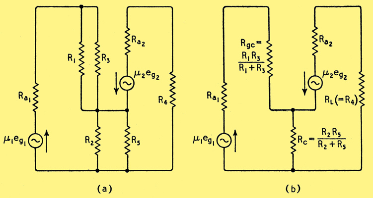
Fig. 6. The equivalent circuit of Fig. 4 can be drawn in the forms shown at (a) and (b).
The degree of asymmetry between e01 and e02 must be regarded as of even greater importance than mere gain. Inserting numerical values in Expression (4) of the Appendix we obtain e01/e02 = 0.989.
The inherent unbalance is less than 1.2% and therefore completely negligible. It may be wondered why any asymmetry should exist in the system; however, a consideration of the equivalent circuit of Fig. 6(b), shows that the sum of the alternating anode currents flows in the cathode load whereas the anode current of V2 alone flows in the anode load. The ratio of the alternating components of the anode currents of V2 and V1 is, however, very large.
Design Considerations
The circuit was specifically developed to drive valves of the PX25 class, and the values are therefore chosen to give a large peak output rather than maximum gain. If it is required to drive valves requiring a smaller grid swing no doubt much higher values of gain can be achieved. It should be pointed out to those evolving their own designs that the dynamic load on V1 is very much greater than the DC load, while the AC load on V2 is less than the DC load.
For smaller output voltages, say up to 25 V RMS at each output point, the component values are not critical while other types of valve have been substituted with only minor circuit changes; e.g., bias and screen resistors. It is of interest to note that the EF36 strapped as a triode gave better results from a linearity point of view than any of the triodes investigated.
As with most cathode-follower systems, it is advisable to reduce the heater-cathode voltage of V2 by using a separate heater supply for the stage, connected to an appropriately decoupled point on the HT supply.
In order to avoid loss of gain it is desirable to by-pass the cathode bias resistors of each stage.
Table 1 gives the results obtained with the circuit of Fig. 4.
Table 1
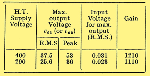
It will be noted than the measured gain is somewhat less than the calculated value, the discrepancy is not however more than can be accounted for by variations in the actual values of components from those assumed.
Application of Circuit
The circuit has been used over a number of years in a wide variety of amplifiers and has proved to be remarkably stable and free from undesirable traits.
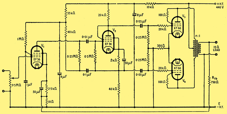
Fig. 5. The circuit of a complete amplifier including the output stage. Overall negative feedback is used.
A complete design is given in Fig. 5. KT66 valves strapped as triodes have been used in the output stage, this method of connection giving a performance roughly equivalent to that of the PX25 type with the added advantages of shorter grid swing, indirectly-heated cathodes and octal base.
Without negative feedback an output of 14.5 W is obtained with less than 0.025 V (RMS) input. If negative feedback is applied as shown in Fig. 5 the required input voltage for maximum output is raised to 0.25V (RMS). The negative feedback reduces the distortion content to 0.5% at maximum output, while the output impedance becomes 120/n2 Ω. It is illuminating to note that this latter value is less than that obtained by operating the same valves as a cathode- follower stage. Using a good quality output transformer the response, with overall negative feedback, was measured to be within ± 1 db from 25 - 20,000 Hz. If an output transformer of poorer quality is used the degree of feedback may have to be slightly reduced in order to satisfy the Nyquist stability criterion.
Where a greater output is required the KT66 valves can be operated as tetrodes in the normal manner and 35 W can then be obtained. The author favours however the use of four valves operating as triodes in parallel push-pull where a large output is desired.
No originality is claimed for the circuit, as a search of the literature has shown that it appeared in the USA some years ago; however, so far as the author is aware no analysis of the circuit has previously been published.
Appendix
|