|
Part three: Extension of Output Voltage Range
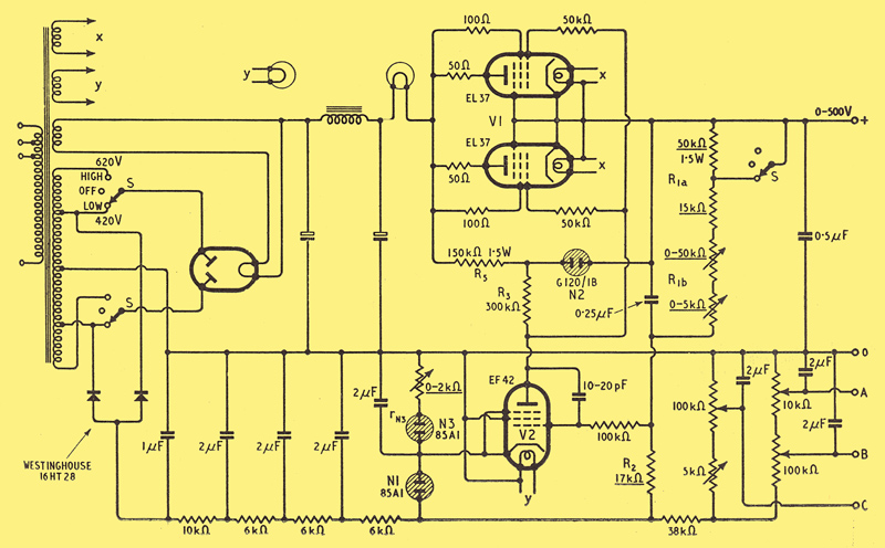
Fig. 13. Modification of Fig. 7 to provide output voltage variable over the range 0-500 V. The resistors underlined at least, should be wire-wound. The outputs obtainable from the negative terminals are:-A, 0 to -9 V, or fine control of B if shorted to 0; B, -9 to -100 V, or 0 to -100 V with fine control if A shorted to 0; C, 0 to -100 V with fine control.
We come lastly to the problem of extra-wide ranges of output voltage. Maximum Vo can be extended in the upward direction by increasing the supply voltage and the maximum value of R1; but, as the working-out of a design with the aid of Fig. 4 showed, unless the minimum Vo is raised equally it is necessary to provide series valves capable of greater anode dissipation. Alternatively, and more economically, the full range of control can be split up into two or more bands by means of a switch controlling E. (the source voltage) and R1a simultaneously in steps. The value of R6a if used, ought also to be changed, but in practice it will be found that when R1a considerably exceeds R2 the error due to omitting R8a altogether is unimportant.
Lowering the minimum Vo is less straightforward. As we saw in Part 1, the limiting condition with the circuit considered until now is that Vo must be sufficient to supply VN1, V2a and V1g1 (max) in series. The lowest available VN1 is about 500 V; V2a can hardly be reduced below 20 V, and in our example V1g1 (max) was 66 V, making 140 V about the lowest practicable Vo. Further reduction, down to perhaps 100 V, could be obtained at the expense of range of Vo control.
For some purposes, however, it may be desirable to extend the range down to zero volts. This can be done by providing a source of negative potential for V2. Such a source can conveniently be made to add still further to the facilities of the unit by providing an external grid bias supply.
Although the modification to the circuit is fairly obvious in principle, there are a number of practical details that require care and attention. These will be discussed with reference to Fig. 13, an extension of the previous design, to cover 0-500 V in two equal bands.
Since N1 cannot be fed from the main stabilized output it is necessary to consider very carefully the effects of its AC resistance. Any voltage variations across it are amplified perhaps 2,000 times and injected into the main supply, and are not reduced by feedback. The most effective way of avoiding them is to stabilize the auxiliary negative supply, but this is somewhat elaborate, necessitating a separate transformer HT winding, valves, etc.
The alternative is to smooth the negative supply very thoroughly. It should be noted that while hum can be reduced by reactances, slow fluctuations in mains voltage are reduced only by series resistance. It is therefore necessary for this resistance to be high. The supply in Fig. 13 is taken from 420 V tappings on the mains transformer, using a pair of Westinghouse 16HT28 metal rectifiers. The 620 V tappings, with appropriately rated components, would be better still. Current in this supply should be kept as small as possible, the requirement for large smoothing resistance overriding the rectifier maximum rating of 15 mA. The reservoir capacitance is limited by the rectifier rating to 1 μF.
The effect of the resistance between screen grid and cathode of V2 is quite different in this circuit. It forms one arm of a bridge, the others being VN1 R2 and R1 (completed by the negligible Ro). V2 (grid to cathode) is the detector, and the negative supply is the signal source. To eliminate the-effect of slow fluctuations in the latter completely, therefore, it is only necessary to make Rg2-k = VN1R1/R2. Such a resistance, being quite insufficient to supply V2g2 must be supplementary to a tube N 3; 0-2 kΩ would usually do.
Unfortunately the value of Rg2-k alias VN3 needed to balance the bridge varies directly with R1 which in this type of unit obviously varies a lot. It can be ganged with R1b and the voltage range switch; a rather elaborate device which may incline one more favourably to a stabilized negative source. This balance is rendered ineffective for hum and other rapid fluctuations by the capacitor across R1. A balancing capacitor across VN3 would have to be very large, and in practice it has been found better to apply most of the available capacitance in the hum filter. Some is useful across N3, however, to suppress random noise.
Since the fluctuations in the un-stabilized negative source correspond only partially with those in the main supply, adjustment of VN3 is not very effective for neutralizing Ri and still less Via. Fig. 10 can be applied successfully, but Figs. 11 and 12 (Part 2) are not directly applicable. Hogg has suggested a modified form in which R7 is inserted in the negative main supply as before, while in place of R2 there is a potential divider across the negative source. The parallel resistance of the two resistors composing it must be equal to R2, and their individual values such as to apply the correct standing V2g1. Changes of VR7 are thus passed to the control grid, but R7 has to be several times greater than in Fig. 11 to allow for the step-down in potential. Moreover the current to be supplied by the negative source is considerably increased. It was considered that these drawbacks were not outweighed by the advantage of separate current feedback, especially as Fig. 10 can be adjusted to do the same thing more simply, though at some slight loss of mains voltage stabilization.
Connecting the heater of V2 to cathode was found to introduce about 10 mV of hum, which could be avoided by transferring it to the zero volts line. If N3 has a tendency to go out when Vo is adjusted towards zero it is because the anode of V2 is 'bottoming', causing I2g2 to increase sharply. The tendency can be reduced by increasing IN3 or preferably by removing the cause such as by reducing Vi or increasing R5.
The procedure for calculating resistance values, etc. is the same as for Fig. 7. The grid bias scheme calls for no comment, except to point out that the outlets are not to be used for supplying appreciable current.
The voltage range switch ought, of course, to be capable of safely handling the high voltages, up to about 1,750 V peak, across the transformer outers. One of the old-fashioned anti-capacity types, slightly modified to increase the leakage paths, has been found satisfactory.
It can be seen from all this that the facility of voltage control below 100-200 V necessitates considerable elaboration of the unit and reduces the possibilities of obtaining a high degree of stabilization. By accepting some restriction on the output current and the regulation, one or more output voltages, variable down to zero, can be obtained quite simply as additions to the main highly-stabilized output.
Part 2 Appendix
|