|
Design of a Triode Amplifier
Now we shall design an amplifier from square one and see how it stands up to a practical test. The valve that we shall use is the ECC81, which we now know is the same thing as a 12AT7, or even a CV455. Since this comprises two triodes in a single envelope, we shall only need to use one of them, at least initially.
It would be nice if the design of an electronic circuit could be carried out merely by using a set of formulae into which we inserted the required parameters for performance, and out came all the component values! Unfortunately, life just isn't like that and there is usually an element of 'guestimation' somewhere in the design, often at the beginning. For example, supposing that we know that we need to amplify a certain signal by 20 times, how do we proceed to design an amplifier using this single fact? What DC supply voltage should be applied to the stage? What should be the value of the anode current? Where do we place the grid bias point on the mutual characteristic? In short, where do we start? Where we start is dictated largely by common sense, though a little previous experience helps as well. Take the question of the supply voltage; this may well be dictated by the availability of an existing power supply. However, we should also consider how large the output signal can be, since this may influence the choice of an alternative DC supply. Let us take an example. The circuit for the amplifier that we are going to design is shown in below.
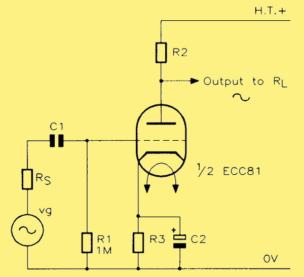
Basis for the design: circuit diagram for a single-stage triode amplifier.
It is a simple, single-stage voltage amplifier, which is assumed to be fed from a source of some impedance Rs, and whose output is to drive a load Rl. In this design we shall have to determine the values of the anode load and cathode bias resistors, R2 and R3 respectively, as well as the value of the input coupling capacitor C1 and the cathode bypass capacitor C2. The grid leak resistor Rl has the usual value of 1 MΩ.
If we are using the simple valve power supply presented in A Valve Power Supply, then the available DC output voltage will be approximately 150 V, and the amplifier design will have to take that into account as a limiting factor. Suppose that we know that the signal source will never provide a signal greater than 0.6 V RMS in magnitude. If the gain of the amplifier is 20 times, then the output voltage from the amplifier can never be greater than 0.6 x 20 = 12 V RMS. This we must convert to a Pk-to-Pk value in order to see how the signal swings fit in with the limit of 150 V total dictated by the power supply.
The relation between RMS value and the corresponding Pk-to-Pk value is given by:
Pk-to-Pk value = RMS value x 2√2 or 2 x 1.414
Which in this case means that the Pk-to-Pk output voltage
= 12 x 2.828,
= 34 V (approx.)
= 17 V peak.
This is apparently well within the range of the 150 V supply to be used. All we need do is ensure that the steady (no signal) value of the anode voltage allows the total swing of 34 V to take place without either signal peak approaching too closely to either 0 V or + 150 V. The easy solution is to set the steady anode supply voltage halfway between 0 V and the HT value, namely 150 V. This would give a steady anode voltage of 150/2 = 75 V. On positive half-cycles of the signal, the output level would rise to 75 + 17 V, which equals 92 V; on the negative half-cycles of the signal, the output level would fall to 75 - 17 V, which equals 58 V. Quite clearly there is a healthy margin in hand in terms of the voltage gap between each peak and the appropriate supply rail, as shown.
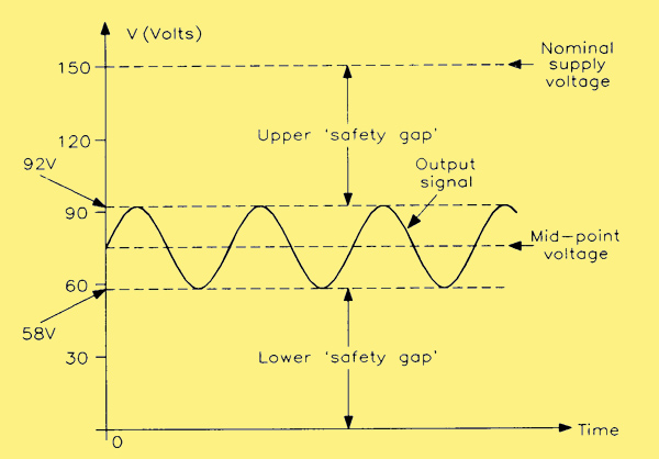
An essential step in amplifier design: setting the DC operating point. Choice of the mid-point ensures maximum symmetry of output but other settings are possible.
This should always be integral to any amplifier design. It might be tempting to assume that, in the case of this particular design, where the anode voltage is set midway between 0 V and HT +, that we could actually drive the amplifier so as to produce an output swing of 75 V peak, the anode voltage then rising to + 150 V on one half-cycle and falling to 0 V on the other. This is only theoretically possible however, the difference between theory and reality being that non-linearity of the valve characteristics would cause gross distortion to be produced well before these limits were reached.
It is not always either necessary or desirable to set the steady value of the anode voltage to half the supply voltage, just to ensure that the signal can be accommodated. As long as the signal swing does not closely approach either HT + or 0 V, a wide range of values for the choice anode voltage is possible. In particular design we shall set the value at about 100 V.
Calculations for the Anode Current and Anode Load
The steady value of the anode voltage is equal to the supply voltage minus the potential drop across the anode load resistor. Mathematically:
Va(DC) = VHT - (Ia x R2) - (Equation One)
If we substitute the known quantities into the above equation, we get:
100 = 150 - (Ia x R2)
The second term on the right-hand side, i.e. the product of anode current and anode load resistor, is unknown, or at least one of the terms within it, either Ia or R2, is effectively unknown, since knowing either of these would allow the other to be found by transposition! The question is, which one can be turned into a 'known' term?
One parameter that has been defined for this amplifier design is the voltage gain, which is required to be 20. The formula for voltage gain, or Voltage Amplification Factor (VAF) as it is alternatively known, for a triode is as follows:–
VAF = (μ x Rl) / ra + Rl - (Equation two)
The values for the above parameters for the ECC81 are typically ra = 13.5 kΩ μ = 54 at an anode voltage of about 170 V, rather higher than that used in this design. We can, at least initially, substitute these values into the equation for VAF, as well as the required value of VAF, namely 20, to give:
20 = (54 x Rl) / (13.5 + Rl) - (Rl and ra both in kΩ)
Transposing and simplifying, Rl = 270 / 34 = 7.94 kΩ
You may be saying at this stage that what we are interested in finding is not Req but R2, the anode load resistor. Yes, that is true, but in this design they are assumed to be the same thing. Since the load which the amplifier is driving is high, it has negligible shunting effect on the anode load and, hence, on the voltage gain. We can consider other cases later.
We should probably choose to use the nearest preferred value to the above calculated one, namely 8.2 kΩ, even though, in theory, this would give a gain slightly higher than that required. However, this is not of any real importance, since there is no guarantee as to the actual value of gm that the valve in use will have anyway, because the figure of 4.0 mA/V quoted in the data book is no more than a guide to the typical value, and production tolerance spreads will ensure that some samples will lie above this value and some below. In fact, I decided to use a 10 kΩ resistor for the anode load thus, hopefully, giving me a little gain in hand. You may get some flavour of how design goes in practice from this: you just cannot be too academic about it, because so often there are few parameters that can be tied down exactly, and flexibility and compromise often have to be used. We can now return to Equation one above and substitute into it the value of R2. This gives:–
100 = 150 - (Ia x 10) (Ia is assumed to be in mA)
This must be transposed for Ia to give:
Ia = (150 - l00) / 10, = 5 mA.
This value of anode current is well within the capabilities of the ECC81, as can be seen from the mutual characteristics for this valve given in the diagram below.
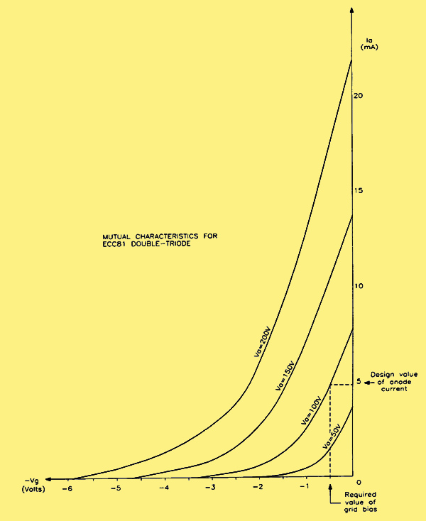
Using the mutual characteristics to determine the grid bias voltage.
Calculation of Cathode Bias Resistor
This is R3 in the circuit diagram at the top of the page, and its value is given by the following Ohm's Law equation.
R3 = (Bias voltage required) / (Anode current)
The value of bias voltage required is obtained from the mutual characteristics above, where the anode current value calculated previously, namely 5 mA, is projected across to the Va = 100 V characteristic and then projected down onto the -Vg axis. The value of Vg required is then found from this construction to be -0.5 V. The value of R3 is easily obtained now by dividing the bias voltage (0.5 V) by the anode current (5 mA) – convenient figures! – to give a value for R3 of exactly 100 Ω.
Decoupling the Cathode Bias Resistor
As is the case with common emitter transistor amplifiers, the resistor in the cathode lead (emitter lead) must be decoupled satisfactorily at all frequencies of interest. The rule-of-thumb method that allows the correct choice of decoupling capacitor to be made is as follows.
'At the lowest frequency of interest, the decoupling capacitor should have a reactance no greater than one tenth of the value of the resistor that it is to decouple'.
Using this rule, and with a bias resistor value of 100 Ω the decoupling capacitor should have a reactance of not more than 10 Ω, at the lowest signal frequency. Let us assume the latter is to be, say, 20 Hz. Using the formula for capacitive reactance, that:
Xc = 1 / (2π x f x C)
the value of C works out to be 796 μF
Rounding this up to 1000 μF should ensure satisfactory decoupling.
The Input Coupling Capacitor
It is fairly common practice at audio frequencies to use a value of about 10 n to 100 nF, usually the latter; on an old circuit diagram this would be marked as a value of 0.1 μF, which is just another way of expressing the same value. However, rather than just make this bald statement, which could even be regarded as something of a get-out, we should justify the value by calculation. Not only will this give us confidence in the choice we have made, but will also provide a basis for making alternative choices, given new criteria, should we want to do so.
The value of this coupling capacitor, C1 in the circuit diagram, is only important at low frequencies. Furthermore, at these frequencies the input capacitance of the valve, being very small, is of no significance and the equivalent circuit of the amplifier input reduces to that shown
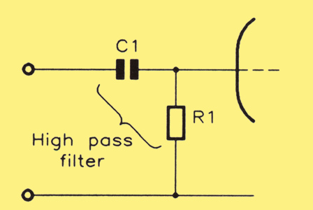
The input circuit of the amplifier as a high pass filter.
which is a high-pass filter comprising C1 and R1. At low frequencies, the reactance of C1 becomes of significance – the lower the frequency, the greater this reactance becomes – and there will be some particular value of frequency at which the reactance of C1 is exactly equal to the resistance of R1. At this frequency and under this condition, the loss of signal between input and output of this filter will be 3 dB. Since this is the usual way to specify the limits of amplifier bandwidth, if we know what the lower limit of band-width should be, we can choose such a value for C1 that no more than 3 dB of signal loss occurs at this frequency.
To take an example, suppose that the lower -3 dB frequency is to be no higher than 20 Hz then, at this frequency, the reactance of C1 should not exceed the value of R1, namely 1 MΩ. Using the formula for capacitive reactance in exactly the same way that we did when determining the value of the cathode bypass capacitor C2, we obtain a relationship as follows:–
1 MΩ = 106Ω
from which
C = 1 / (40π x 106) F = 0.008 μF (approx) = 8 nF
From this result, it is obvious that a value of 100 nF more than meets the bandwidth requirement. This completes the basic design of the amplifier, and it now remains only to hook it up and test it.
|