|
The Triode Amplifier – an Introduction
In general, amplifiers can be classified according to their characteristics and properties. One such classification is according to the frequency range over which they are supposed to operate, and which falls into four broad divisions:–
- direct-coupled amplifiers;
- audio-frequency amplifiers;
- radio-frequency amplifiers and
- video-frequency amplifiers.
Another possible classification may be used to determine whether the amplifier is 'aperiodic' (untuned) or tuned. For example, audio-frequency amplifiers are aperiodic, because they are intended to handle all frequencies in the audio-frequency spectrum equally. Radio-frequency amplifiers, on the other hand, whether in transmitters or receivers, are tuned amplifiers, since they are intended to concentrate on a narrow band of only frequencies centred around a single radio-frequency, often the 'carrier', to the exclusion of all others.
Amplifiers can also be classified as either voltage or power amplifiers, according to whether the primary aim is to raise the voltage level or the power level of a signal. This is true whether the amplification is at audio or radio-frequencies.
Finally, amplifiers can be classified according to their operating conditions, eg, class A. class B, class AB or class C. But for the moment at least we shall consider the use of the triode valve as a voltage amplifier at audio-frequencies.
The Triode as an AF Voltage Amplifier
To understand how amplification is possible with a triode valve, we need to remind ourselves about the mutual characteristics of a triode (the graph of anode current Ia against grid voltage Vg), and of the need for a grid bias voltage and how the latter is obtained. Previously we discussed this characteristic, in particular how it showed that the standing value of anode current through the valve depends upon the negative voltage applied to the grid; if this negative voltage is made sufficiently large, the anode current becomes cut off altogether. We also discussed how the negative bias voltage for the control grid could be obtained by making the cathode positive with respect to the grid, this then being termed cathode bias.
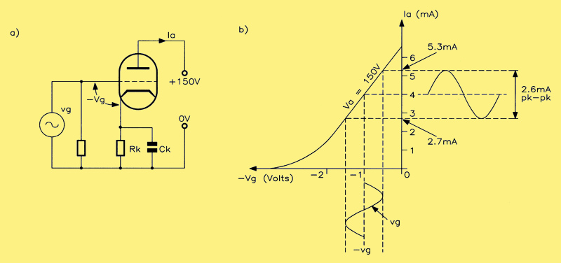
(a) A triode valve with grid bias Vg and an alternating input signal vg: (b) Standing and alternating voltages and currents for the valve of (a)
With the above in mind, now look at (a) and (b) above. Figure (a) shows the triode valve with cathode bias components Rk and Ck, and the grid leak resistor Rg. An alternating input signal (a sine-wave) is applied to the grid; the latter is known as Vg (small 'V') as opposed to Vg which is the DC bias voltage. This situation is shown graphically in Figure (b). The construction shows that, for this particular valve, the value of the bias voltage Vg is -1.0 V, which produces a standing value of anode current Ia equal to 4 mA. This is obtained by projecting upwards from the value of -Vg until we intercept the static curve for Va = 150 V and then projecting across to the vertical axis where we read off the value of Ia, namely the 4 mA referred to. This discussion has only dealt with the DC conditions which are valid in the absence of a signal.
However, the above amplifier has an alternating signal voltage applied to the grid and Figure (b) shows that this has a peak value of 0.5 V. Thus, as can be seen from this figure, the grid voltage swings between the limits of -0.5 V and -1.5 V, this occurring equally on either side of the bias voltage value of -l.0 V. From this we would expect that the anode current would also alternate in a similar manner, increasing on the 'positive going' half-cycles and reducing on the 'negative going' half-cycles. Notice the reference to the 'positive going' half-cycle rather than simply saying positive half-cycle. This is, of course, because the grid never actually becomes positive (with respect to 0 V) but only 'less negative'. The peaks of the alternating grid signal voltage have been projected upwards to intercept the static curve referred to earlier and then projected across to the Ia axis. This gives the limits of the corresponding variation of anode current.
When the grid voltage swings to -1.5 V the anode current falls to 2.7 mA, and when the grid voltage swings up to -0.5 V, the anode current then increases to 5.3 mA, This represents a Pk-to-Pk anode current variation of 2.6 mA, centred about the steady anode current (no signal) value of 4 mA.
So far we have used a voltage variation on the grid to produce a corresponding variation in the anode. That is to say, we have a voltage and a current output. What we for voltage amplification is to have voltage output for a voltage input.
The Anode Load Resistor
Of course, all we need to do to turn current into a voltage is to pass through some passive component which is capable of developing a potential difference. Obviously such a device should be linear if we wish to prevent unnecessary distortion occurring. The choice, naturally, is a resistor. This resistor is inserted in series with the anode supply voltage so that the anode current flows through it on its way to the positive supply terminal. This is demonstrated below.
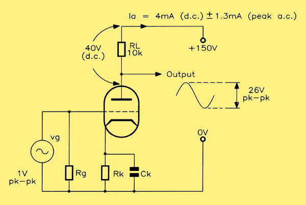
Developing an output voltage by means of a resistive anode load.
There will, therefore, be a potential difference across it, which can be seen to have two components, as follows:–
- A steady voltage equal to the product of the standing current (Ia = 4 mA) and the value of the anode load resistor (in this case, 10kΩ). This product equals 40 V.
- An alternating voltage whose peak value equals the product of the peak value of the alternating anode current (1.3 mA) and the value of the anode load resistor (10kΩ). This product equals 13 V. Thus, by inserting a load resistor in series with the alternating anode current, we have effectively converted the latter into an alternating output voltage of a Pk-to-Pk value of 26 V.
This is clearly much greater than the value of the input signal voltage. By comparing these two values, input and output, we can obtain a figure for the voltage amplification factor (VAF) of the stage.
VAF = (alternating output voltage) / (alternating input voltage)
Obviously we must compare the two voltages specified in the same way, that is, both peak, both Pk-to-Pk or both RMS. We don't know the latter but could calculate it; we know both of the former and one is as good as another for our purposes. Let us use Pk-to-Pk values thus:
VAF = (26.0 V) / (1.0 V) = 26
in other words the voltage gain is 26 times.
General Expression for Voltage Gain
There is a simple expression which can be used to find the voltage gain of a stage such as that shown above. It involves just two factors: the mutual conductance, gm, of the valve, and the 'effective' load in the anode circuit. In the case of this example, the anode load is simply the 10kΩ resistor. In practice, this stage might well feed another, following, one, in which case the anode load resistance of the first stage would be shunted by the input impedance of the second. To take account of such shunt resistances, the effective load is termed the 'equivalent load resistance', denoted by Req. The general expression for voltage gain is then given by:
VAF = gm x Req.
We ought to be able to use the above expression to confirm the voltage gain value obtained graphically in the previous example. The value of Req is clearly just 10kΩ, since there is no following stage attached. Okay. The next question is, then, what is the value of gm? If we knew the valve type, we could simply look up the typical value of gm in a valve data book. However. we will instead obtain it in a way that will make use of the theory given earlier in the series – a much more useful if more lengthy procedure!
The gm of a valve can be obtained by measuring the slope of the mutual characteristic. This measurement should be made at the operating point, that is the portion of the characteristic at which the valve is seen to be DC biased. in this case, defined by Vg = -1.0 V; Ia = 4 mA. The mutual characteristic of Figure (b) at the top of the page is now repeated below with the appropriate construction added as follows:–
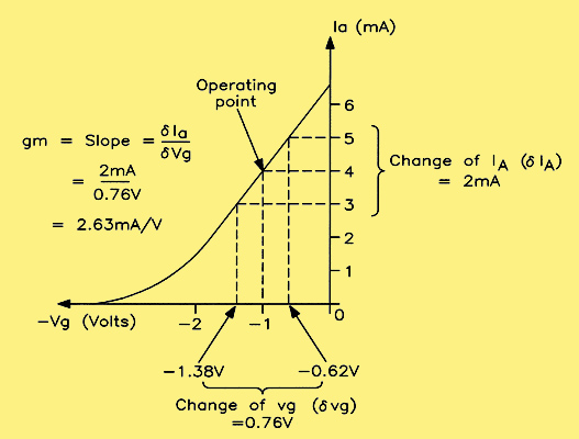
Determining the gm of a triode valve.
A graph has been drawn with convenient increments of anode current, Ia. in the vertical Y axis; in this case the increments of Ia are 1 mA on either side of the standing quiescent value of 4 mA. i.e. total change of Ia (delta a) of 2 mA. Note use of Greek letter delta, also often used to describe the triangular shape outlined by the dotted lines in the diagram above,thus identifying that these are not the static DC biased values we are dealing with. All we need do now to find the value of gm is to project this variation delta Ia downwards onto the horizontal Vg axis to find the corresponding change in Vg (delta Vg). Dividing the change in Ia (delta Ia} by the corresponding change in Vg (delta Vg} yields the mutual conductance gm.
Since the increment in Vg is from -0.62V to -1.38V. then the total change in Vg is 0.76 V giving a value for gm of 2 mA / 0.76 V. which equals 2.63 mA/V. A perfectly reasonable value for a triode. We are now in a position to calculate the voltage gain of the stage.
As stated previously. VAF = gm x Req
where gm = (delta Ia) / (delta Vg)
VAF = 2.63 (mA/V) x 10 (kΩ) = 0.00263 (A/V) x 10,000 Ω = 26.3.
This is the figure obtained previously, thus pointing to the validity of the formula used. Note that the product of gm in mA/V and load resistance specified in kilohms will give the correct numerical value, a useful fact which avoids the use of the appropriate powers of 10 (since these are implicit as in the method of the second line above).
The Triode Parameters
We have now met two of the three triode parameters, namely the anode slope resistance ra, and the mutual conductance gm. The third of the parameters is μ (mu) and is known as the 'amplification factor'. This is NOT the same thing as the Voltage Amplification Factor (VAF) referred to above. μ is a parameter of the valve itself, and has no relation to the value of anode load used. VAF is the voltage gain of an actual stage and is dependent upon the value of anode load used. It is not surprising that the value of VAF will always be somewhat less than the value of μ, since there will always be some signal loss due to the fact that the valve amplifier has some internal resistance (ra in fact). What μ does give us is a clue to the ability of any given valve to act as a voltage amplifier – a starting point for a design, if you like. There is a simple relationship between the three valve parameters, by which anyone can be calculated if the other two are known. This relation is:–
μ = ra x gm
Taking a real example, the entry in the table below for the ECC81 shows that ra = 13.5kΩ and gm = 4 mA/V.
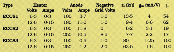
Principal parameters of ECC81, ECC82 and ECC83 double triode valves. For an understanding of how Mullard/Philips named receiving valves see here.
These two figures can be multiplied together directly to give the amplification factor μ. Thus, &mu' = 13.5 x 4, = 54. This is the value given in the table. There are, of course, no units for μ since it is a ratio of output voltage over input voltage (signal values). This can be seen from a simple multiplication, as follows:
ra = (change of Va) / (change of Ia)
gm = (change of Ia) / (change of Vg)
If we multiply these two expressions together, to get an expression for μ we shall end up with the expression,
μ = (delta Va) / (delta Vg) since the (delta Ia) term will cancel out in both expressions.
Frequency Response of Triode Amplifier
The bandwidth of an amplifier is conventionally defined as being the range of frequencies lying between the two points, where the response has fallen by 3 dB from the mid-band value. At high frequencies the response is limited by shunt capacities, such as the inter-electrode capacity between grid and cathode (known as Cgk). This latter is an obvious 'stray' capacity in parallel with the signal path. What is not so obvious is that this value of input capacitance is enhanced by a further shunt capacity which is 'reflected back' to appear in parallel with Cgk. This additional capacity has a value equal to Cag (the capacitance between anode and grid) multiplied by (approximately) the voltage gain of the stage; this is termed 'Miller effect'. Thus, the input capacitance can actually be quite high, and this sets a limit on the high-frequency performance of triodes, unless special measures are taken to improve this aspect of performance.
The response at the low-frequency end of the spectrum is largely determined by external factors, namely the high-pass filter formed by the series coupling capacitor and the input resistance of the valve. The latter is apparently infinite, because the input circuit of the valve itself is a physical gap between the cathode and grid, with no current flowing in the grid circuit. However, the grid leak resistor appears in parallel with the grid-cathode path and, since this usually has a resistance of 1MΩ, this becomes the input resistance of the amplifier. The frequency response at low frequencies is then determined by the value of the series coupling capacitor.
With a simple RC filter of this type, the -3 dB response point occurs when the reactance of the capacitor equals the value of the resistor. This makes it easy to calculate the value of capacitor required in order to obtain any given low-frequency response. Let us take an example.
Suppose that the grid leak does have a value of 1MΩ and that the lower -3 dB response point is to be at 40 Hz. This means that the reactance of the coupling capacitor must have a value of not more than 1MΩ at this frequency. Thus, since
Xc = 10-6 Ω and Xc = 1 / (2π x f x C)
Then; C = 1 / (2π40) μF = 0.004 μF = 4 nF
This illustrates how the high input impedance of valves allows small values of coupling capacitors to be used. In a solid state amplifier using Bipolar Junction Transistors, coupling capacitors are more likely to have values of the order of lO μF or so (since the input impedance of a common emitter amplifier is of the order of only 2 to 3kΩ). In practice, valve audio-frequency amplifiers in the past commonly used coupling capacitors having values of, say, 0.1 μF (100 nF), which is plenty enough.
|