|
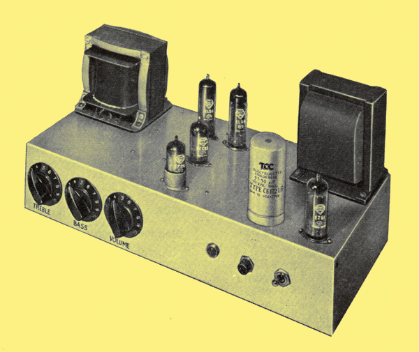
Prototype of ten-Watt amplifier with controls. See also here.
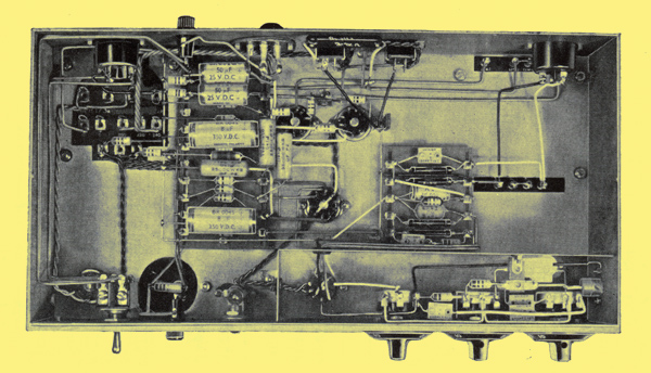
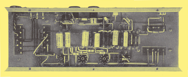
Underside of prototype with controls.
An easily constructed three-stage amplifier with a rated power reserve of 10 W is described in this article. The circuit diagram is below. Several versions of the amplifier are possible. The equipment can be constructed to include volume and tone controls, when it is suitable for direct use with high-level signal sources, or it can be made without controls to be used with pre-amplifying equipment. In addition, three arrangements of the output stage are possible: normal loading, low loading and distributed loading.
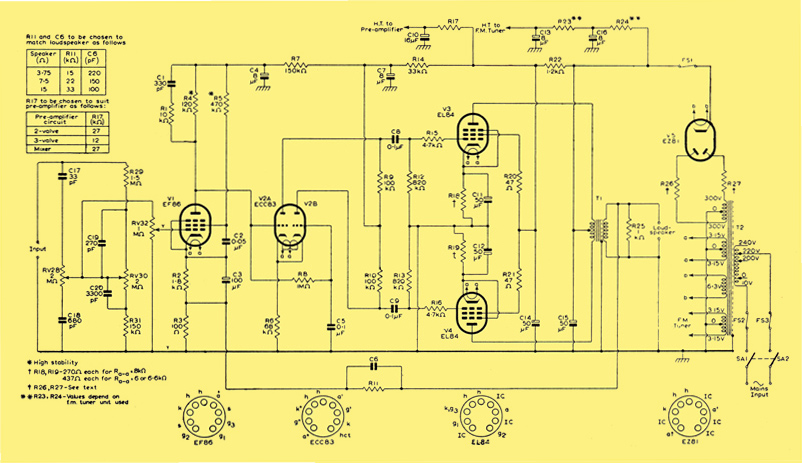
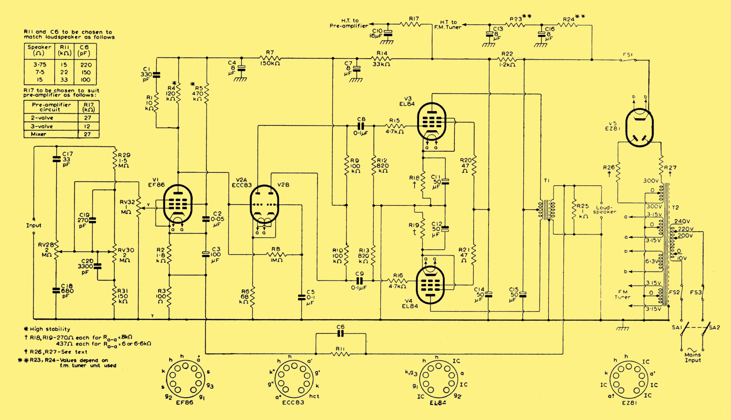
Circuit diagram of 10W amplifier. (For version without controls, the signal is taken directly to the control grid of V1, and RV32 is replaced by a fixed resistance of 1 MΩ
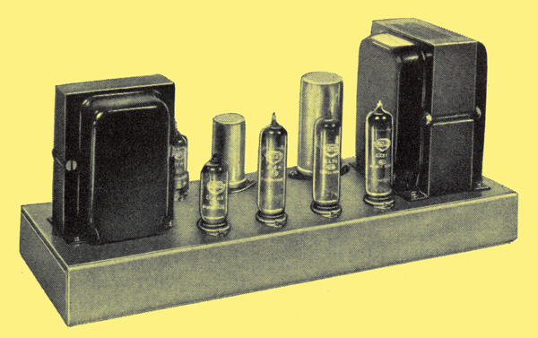
Prototype of ten-Watt amplifier without controls
Underside of prototype without controls
The push-pull output stage of the circuit uses two Mullard output pentodes, type EL84. These yield a rated output power of 10 W with a level of harmonic distortion under normal loading conditions, of less than 0.3%.
The intermediate stage consists of a cathode-coupled phase-splitting amplifier using the Mullard double triode, type ECC83, which is preceded by a high-gain voltage amplifier using the Mullard low-noise pentode, type EF86. The intermediate and input stages are coupled directly to each other so that low-frequency phase shifts are minimised.
The optional treble and bass tone controls are shown in the circuit diagram. RV28 provides continuously variable treble control from +10 to -10 dB at 10 kHz and RV30 provides bass control from +11 to -5 dB at 20 Hz. The level of feedback taken from the output transformer to the cathode circuit of the input stage is 26 dB. The basic sensitivity of the circuit with this amount of feedback is 40 mV for the rated output power, and the sensitivity when the tone controls are included is 600 mV. The level of noise and hum is at least 75 dB below 10 W.
The rectifier used in the power-supply stage is the Mullard full-wave rectifier type EZ81.
Circuit Description
Input Stage
The first stage of amplification is provided by the EF86 in a circuit giving a voltage gain of about 150 times. The negative-feedback voltage from the secondary winding of the output transformer is introduced across the 100Ω resistor R3 in the cathode circuit. Because of the high gain in this stage, any excessive noise will lower the quality of the output from the speaker considerably and so high-stability, cracked-carbon resistors are used for the anode and screen-grid circuits. The EF86 is coupled directly to the phase splitter to reduce the phase shift at low frequencies. A CR network (C1, R1) shunting the anode load produces an advance in phase which increases the stability of the amplifier at high frequencies.
Intermediate Stage
The double triode type ECC83 is operated as a cathode-coupled phase splitter to provide a push-pull drive voltage for the output stage. The use of the cathode-coupled arrangement gives low distortion and facilitates direct coupling with the input stage. The voltage gain obtained with a cathode-coupled circuit is approximately half that obtainable from each valve section operated as a normal voltage amplifier. Nevertheless, it is sufficient because the amplification factor of the ECC83 is 100.
It is necessary in a cathode-coupled phase splitter for the anode load of the earthed section to be slightly higher than that of the first section if perfect balance is to be obtained. Thus R10 should ideally be slightly higher than R9, by a percentage which depends on the amplification factor of the valve. Because of the high amplification factor of the ECC83, nominally equal resistors, matched to within 5%, cannot give rise to more than 2% lack of balance.
At low frequencies, the presence of C5 and R8 in the grid circuit of the second triode section produces both phase and amplitude unbalance. The frequency at which the lack of balance becomes significant depends on the time constant C5 R8, which should be as long as possible to provide maximum decoupling within the pass band of the amplifier. Adequate balance can easily be maintained in practice and the component values used in this circuit give it down to low audible frequencies.
The anode voltage of the EF86 determines the operating conditions of the phase splitter and, provided the values of the associated components are within the stated tolerances, the stage will operate correctly. If the anode voltage of the EF86 is too high, the bias on the phase splitter will be too low and grid current distortion, resulting from overdrive on peak signals, will occur. If the anode voltage is too low, the phase splitter bias will be too high, and the stage will operate away from the linear position of the valve characteristics with a resulting increase in distortion.
Output Stage
The output stage consists of two output pentodes, type EL84, in a cathode-biased, push-pull circuit. The anode supply voltages are taken from the reservoir capacitor C15, while the supply voltages for the screen grids and for the rest of the amplifier are taken by way of R22 and C14.
Compensation for the slightly different currents drawn by any two EL84 is achieved by using the separate cathode resistors R18 and R19. Matching of the output valves is therefore unnecessary.
The stopper resistors R15 and R16 in the control-grid leads and R20 and R2l in the screen-grid circuits have been included as a normal measure to prevent parasitic oscillations. These resistors should not be bypassed, and a close connection should be made to the tags on the valve holders.
A resistor R25 having a value of about 1 kΩ may be placed across the output terminals to prevent instability from occurring when the loudspeaker is disconnected.
Operating Conditions-Normal, Low and Distributed Loading in Output Stage
Three ways of operating the output stage are possible. These use the conditions for normal loading, low loading and distributed loading.
Normal or low-loading conditions are determined by the choice of value for the equal cathode resistors R18 and R19 in the circuit diagram. For normal loading, the value of each resistor should be 270 Ω and for low loading it should be 437 Ω (that is, 390 Ω +47 Ω). The conditions for distributed loading are achieved by including part of the anode load (that is, part of the primary winding of the output transformer) in the screen-grid circuits of the valves.
Normal loading is used when the amplifier is to be tested up to a full output power with a sine-wave input. Low loading is used only with speech and music signals when it gives reduced distortion. Distributed loading conditions are used to achieve a compromise between the performance of the two EL84 when connected as triodes and as pentodes. A sufficient power reserve is maintained, yet distortion is much less than with the usual pentode connection.
Normal and Low Loading
The normal loading conditions correspond very closely to the recommendations for class AB operation of the EL84. The difference is that, in the circuit diagram, separate cathode resistors Rl8 and Rl9 (each equal to 270 Ω) are used instead of a shared resistor of 130 Ω The anode-to-anode load resistance for these conditions is 8 kΩ and the anode current for zero input signal is 2 x 36 mA.
The low-loading adjustment is so called because, with the increased values of cathode resistance, the anode-to-anode load resistance is reduced to 6 kΩ and the quiescent current to 2 x 24 mA. Although the output stage is connected for cathode-bias operation, operation with speech or music input signals approximates very closely to fixed-bias conditions. A comparison has been made in High Quality Amplification between the distortion in the output stage when speech or music signals are used with normal and low loading conditions and this comparison is shown in the article. The distortion curves in that article are for the output stage only. Distortion in the complete amplifier is discussed below.
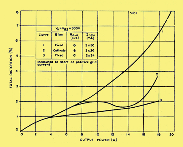
Variations of distortion with output power for two EL84 in class AB push-pull
Curves 1 and 3 in the figure (reproduced above) have been plotted for fixed bias conditions. Curve 1 shows that distortion increases seriously above 10 W when normal loading is used. Curve 3 is for low loading and illustrates the lower level of distortion to be achieved with this adjustment. Curve 2 has been plotted for cathode bias and therefore refers to a sine-wave input. The curve is for normal loading because this is required for sine-wave testing up to the maximum output.
With speech or music inputs, the maximum rated power of the amplifier is only required in the output stage for a small part of the time, the average requirement being comparatively low. However, a large power reserve must be available to cater for the widely differing sound levels which can occur.
The HT current consumption is smaller when the output stage is adjusted for low loading. Consequently, the standing dissipation in this stage is reduced from 11 W at each anode with normal loading to 7.5 W at each anode. The valves are thus being run well below the maximum anode-dissipation rating of l2 W. The HT current requirement is reduced with low loading so that the mains transformer rating can be lower if the amplifier is to be used permanently with the low-loading adjustment.
Larger peak currents are produced in the output stage under low-loading conditions than with normal class AB operation. With speech or music inputs, these peaks are of short duration. They are supplied by the reservoir capacitor C15 which is large enough to provide satisfactory smoothing. When the amplifier is at the point of overload on a peak signal, the momentary fall in line voltage from a nominal value of 320 V should not be more than 2 V.
As the current in the output stage increases, the bias voltages across the cathode resistors also increase at a rate determined by the time constants of the bias network. It is unlikely that this increase will exceed 1 V. The working conditions of the output stage are such that the output valves are driven back into a region where lower distortion is obtained. As a result of this change in bias, a variation in gain will occur, but the distortion introduced by gain variation is held to a low level by the large amount of negative feedback. The total effect, therefore, is to improve the performance at peaks of output power.
It will be realised that, when the amplifier is being used for its primary purpose as a means of home entertainment, the low-loading adjustment is to be preferred to normal loading. However, sine-wave testing up to the full output power should not be undertaken with the low-loading arrangement. Such testing should only be undertaken with normal loading. Measurements of frequency response may be made with low-level sinusoidal inputs provided the output power does not exceed .1 to 1.5 W and square-wave testing may also be undertaken if the signal is again restricted in the same way as the sine-wave input. It is not felt that these restrictions will be of very great significance because few home constructors will have the equipment needed for sine-wave and square-wave testing.
Distributed Load
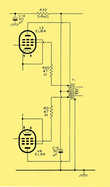
Arrangement of output stage for distributed loading
The arrangement of the output stage for operation under conditions of distributed load is shown. The screen-grid resistors R20 and R21 are disconnected from C14 in the circuit diagram and are connected to the tappings provided on the primary winding of the output transformer. The centre .tap of the primary winding is connected, as before, to the reservoir capacitor C15. The dropper resistor R22 in the HT line no longer carries the screen-grid current and so is increased from 1.2 kΩ to 5.6 kΩ to maintain the same DC conditions in the first two stages of the amplifier.
The best results are obtained with each half of the primary winding tapped so that about 20% of the turns are common to the anode and screen-grid circuits, when the anode-to-anode loading should be 6.6 kΩ.
With distributed loading, total distortion is reduced very much compared with normal loading. The rated power reserve of 10 W is maintained although overloading now occurs at 11 W instead of l4 .W. However, the rate at which distortion increases with output power after overloading is less with distributed than with normal loading. The frequency response of the amplifier is the same for either method of loading, although the stability is improved with distributed loading because the lower level of distortion is obtained with reduced loop gain.
Negative Feedback
The level of negative voltage feedback taken from the secondary winding of the output transformer to the cathode circuit of the input valve is 26 dB. The output impedance with feedback is 0.9 Ω measured at the 15 Ω output terminals. This gives a satisfactory damping factor of about 17 (that is, 15/0.9).
Power Supply
The power-supply stage shown in the circuit diagram uses the Mullard indirectly heated, full-wave rectifier, type EZ81. Adequate smoothing is achieved using the resistor R22 and the large capacitor C15 (50 μF) so that the expense of smoothing chokes is avoided. The current supplied by the EZ81 is sufficient for any arrangement or the output stage and also allows the use of a radio tuner unit. If the low-loading version of the output stage is adopted and it is not intended to use the amplifier with an FM tuner unit, then the Mullard rectifier, type EZ80, can be used in place of the EZ81, but it must be emphasised that currents greater than 90mA must not be taken from the EZ80.
Limiting resistors must be included in the anode circuits of the rectifier, and their values will depend on the type of mains transformer used. The total resistance -made up of the added resistance and the effective resistance of the mains transformer- must be at least 190 Ω per anode for the EZ81 used in this particular circuit (215 Ω for the EZ80). For most 300-0-300 V mains transformers, the effective resistance is about 130 Ω so the value of R26 and R27 (in the 20% range of preferred values) must be at least 85 Ω each (100 Ω for the EZ80). With the power supply giving an HT current of 80 mA the voltage across C15 should then be near the specified 320 V, The voltage across C15 must not exceed 320 V at either 80 mA with normal loading, (Ra-a=8 kΩ) or 60 mA with low loading (Ra-a=6 kΩ}.
When an FM radio tuner unit is used with the amplifier, the additional HT current drawn will not normally exceed 35 to 40 mA and the voltage across C15 will then drop to approximately 295 V. This additional current should be taken from C15 by way of suitable dropping resistors R23 and R24 and should have adequate decoupling (provided by C13 and C16). In these circumstances, the overload point of the amplifier is reduced from 13 or 14 W to approximately 12 W.
The HT supply for pre-amplifiers should be taken from C14. The values of the smoothing resistor R17 given in the circuit diagram are suitable for use with the Mullard designs for two and three valve pre-amplifiers.
Construction and Assembly
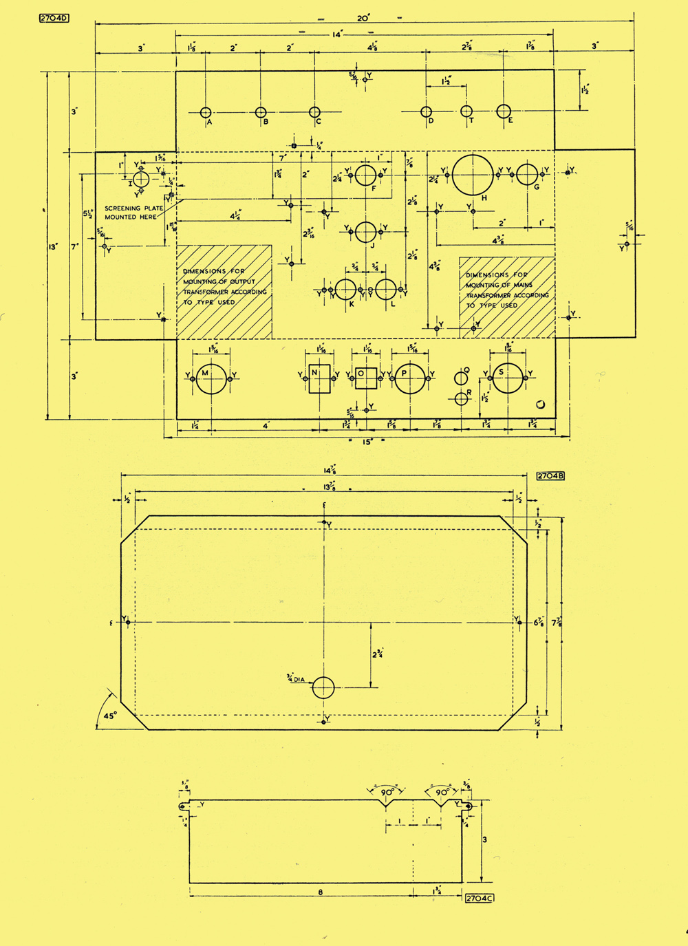
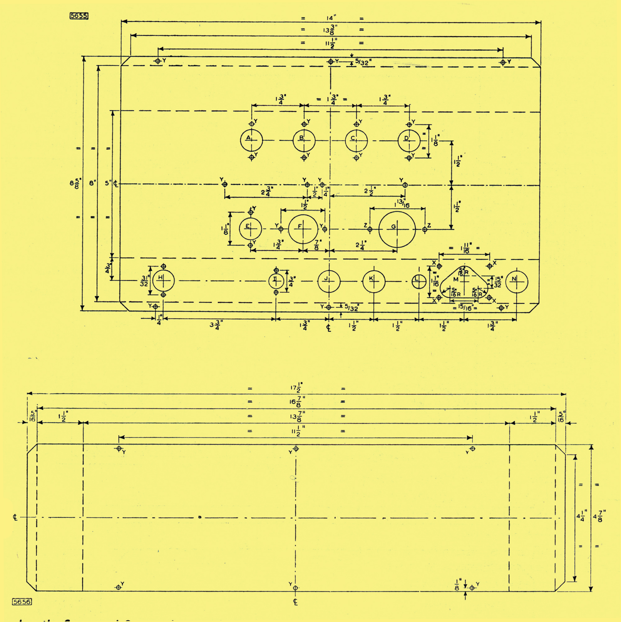
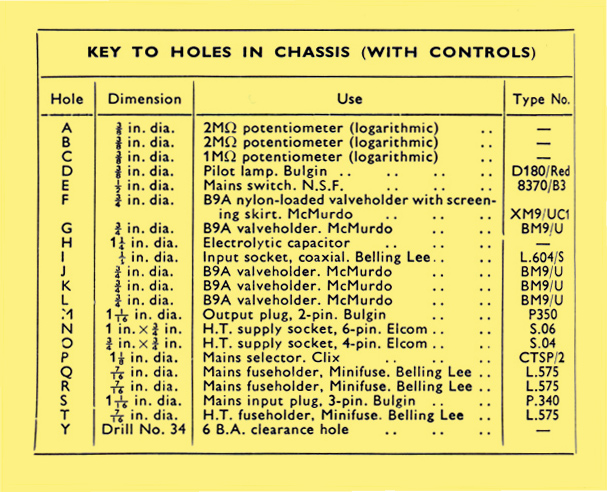
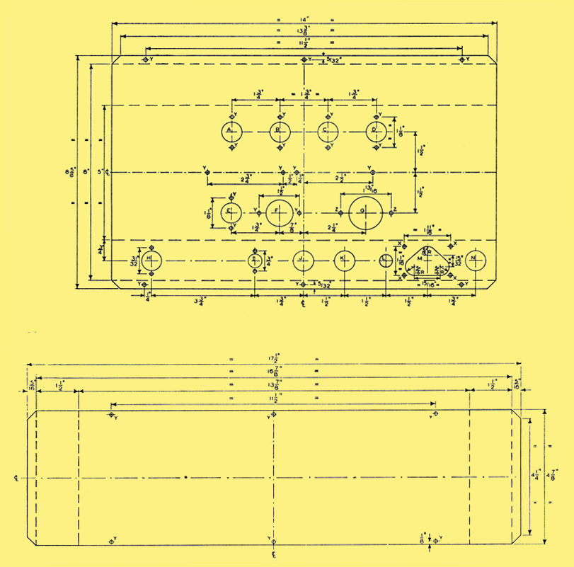
The chassis for the 10 W amplifier in which tone and volume controls are incorporated is made from three separate pieces of 16 .SWG aluminium sheet. Two separate pieces of 16 SWG aluminium sheet are required for the version without the controls. The dimensions (in inches) of these pieces are:–
A For version with controls: (a) Main chassis 20 x 13, (b) Base 14.875 x 7.875, (c) Screen 8 x 3
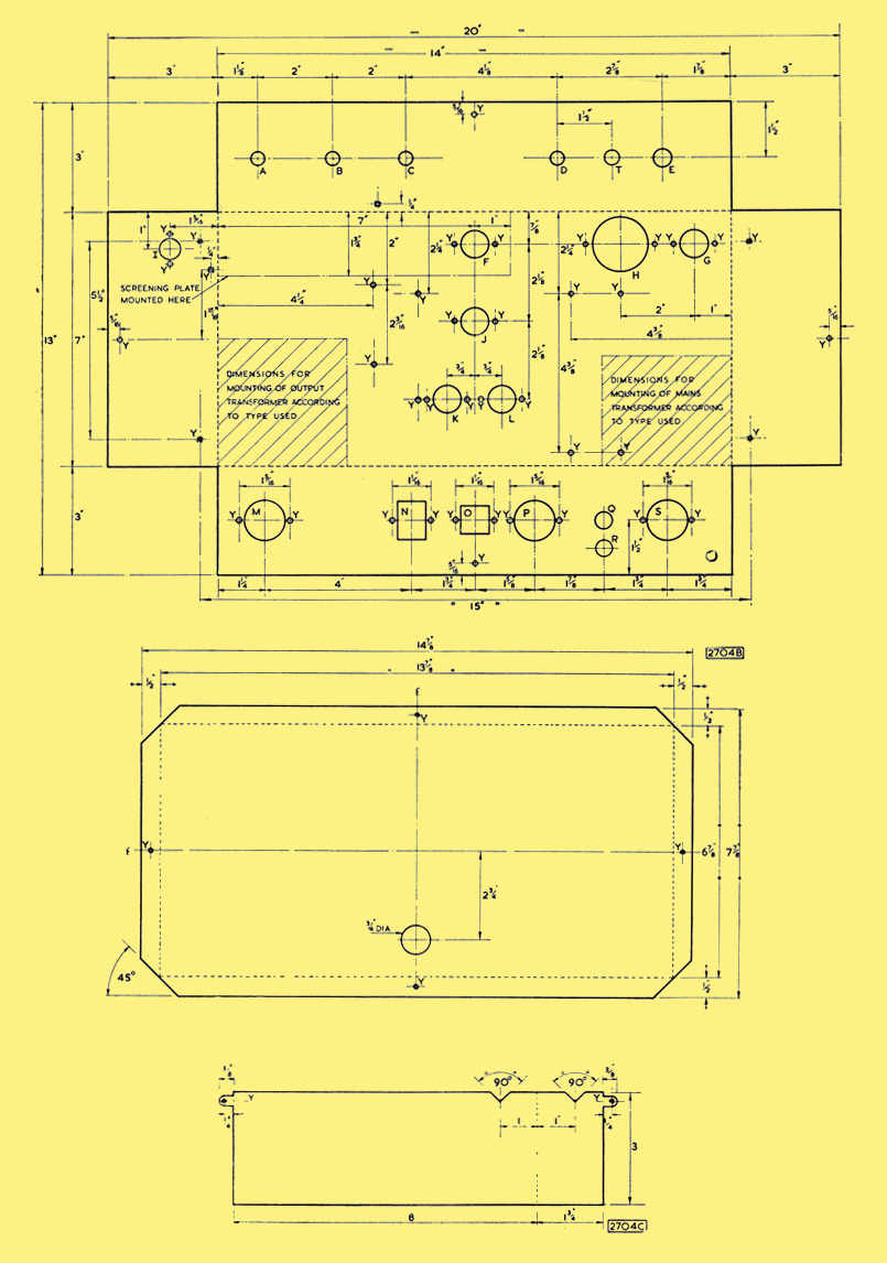
Chassis details for amplifier with volume and tone controls (the sections should be bent up at 90° at all dotted lines. Top - main chassis, Middle - Base & bottom - screen.
B For version without controls: (a) Main chassis 14 x 8.625 (b) Base 17.5 x 4.875.
Chassis details for amplifier without volume and tone controls (the sections should be bent up at 90° at all dotted lines. Top - main chassis, bottom - screen.
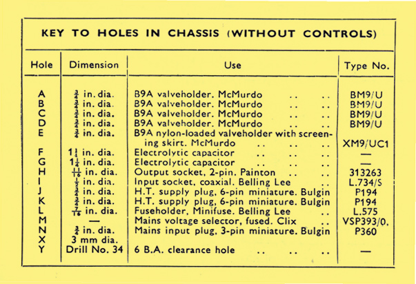
The pieces should be marked as shown in either the upper plan (with controls) or the lower plan (without controls) and the holes should be cut as indicated. Where bending is required, it is important for the bends to be made accurately at the lines for the pieces to fit together properly on assembly. Two sets of assembly drawings are included. One set is for the version of the amplifier which includes the volume and tone controls and the other set is for the control-less version of the amplifier. The versions differ considerably in layout, but the two arrangements will give good stability.
The layout of the control-less version has been dictated to some extent by the requirements of stereophonic equipment. The narrow chassis with the sockets arranged on one side will enable two amplifiers to be used back-to-back with considerable economy of space. A symmetrical arrangement of two amplifiers can be achieved if one of the units is built as a mirror image of the other.
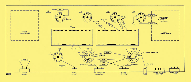
Suggested layout of components for amplifier without controls. (the output stage is connected for distributed loading)
 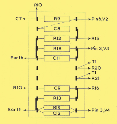
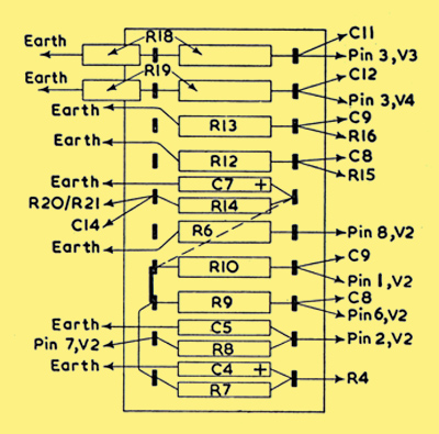
Left: tag-board no. 1 for amplifier without controls. Right: tag-board no. 2 for amplifier without controls
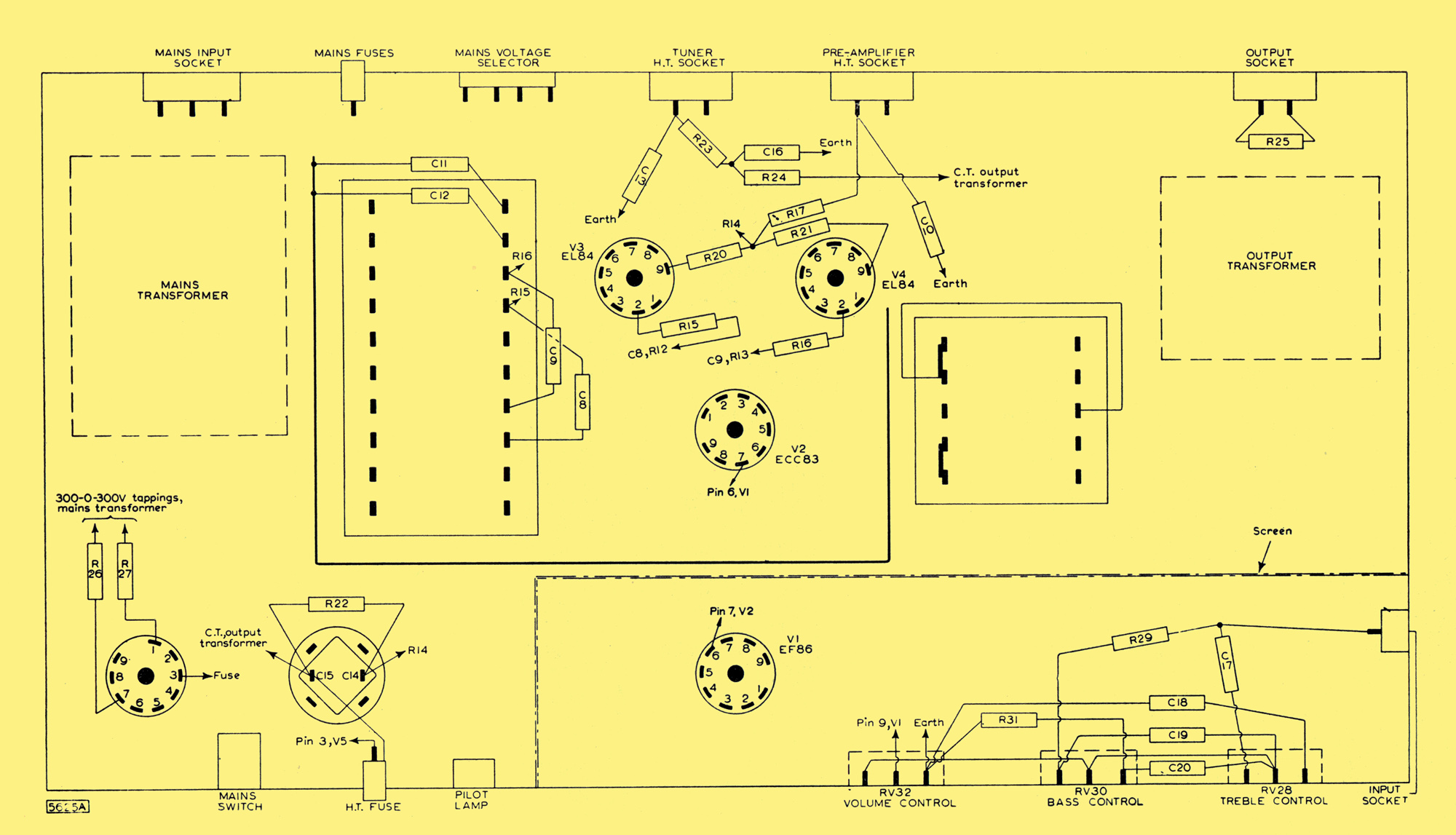
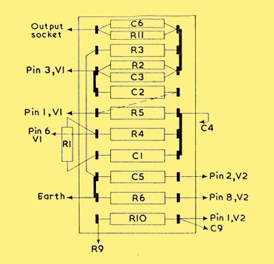
In the version of the amplifier having controls, the majority of resistors and small capacitors are assembled on one ten-way tag-board and one five-way board. These are drawn and presented below. The position of these boards and the other components is shown in the suggested layout, and the wiring between the components is also shown in this figure. A busbar earth return is used and only one connection is made between this and the chassis. This connection is made, via the volume-control potentiometer, at the input socket. The only valveholder which needs to be skirted is that for the EF86, and it should also be nylon-loaded.

Suggested layout of components for amplifier with tone and volume controls
 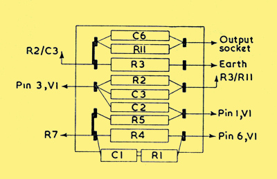
Left: tag-board no. 1 for amplifier with controls. Right:tag-board no. 2 for amplifier with controls
DC Conditions
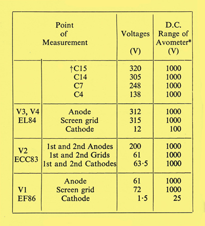
DC conditions.
*Resistance of AVO 8: 1000 V range = 20 MΩ
100 V range = 2 MΩ
25 V range = 500 kΩ
† Alternating voltage at C15 is 4 V for normal loading and 2.5 V for low loading
The DC voltages at points in the equipment should be tested with reference to the above table. The results shown in this table were obtained using an Avometer No. 8 and this has a sensitivity of 20,000 Ω/V
Performance
Distortion
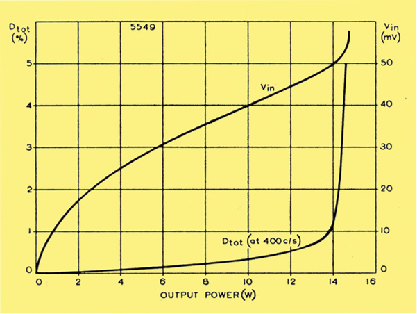
Harmonic distortion and output/input characteristics
The total harmonic distortion of the prototype amplifier with normal loading and with feedback was measured at 400 Hz. The variation with output power is shown above. The relationship between input voltage and output power is also drawn in the above diagram. At the full rated output power, the distortion is less than 0.3% and at about 14 W it rises to 1%.
Measurements of inter-modulation distortion were made in the prototype amplifier using carrier and modulating frequencies of (a) 10 kHz and 4O Hz, and (b) 7 kHz and 70 Hz, the ratios of the amplitudes being 1:4. The values are plotted in the figure below against equivalent output power. For a stated equivalent output power, the peak value of the combined inputs is equal to the peak value of a single sine-wave input which would produce that power. For frequencies of 10 kHz and 40 Hz, the inter-modulation distortion (expressed in RMS terms as the percentage of inter-modulation products relative to the amplitude of the higher frequency) is better than 1.0% at 10 W equivalent output power.
The magnitude of 'beat-note' distortion has been measured with frequencies of (a) 9 and 10 kHz, and (b) 14 and 15 kHz, the amplitudes of the input signals being equal. The difference component present in the output, expressed as a percentage of either signal, is also plotted against equivalent output power and presented below.
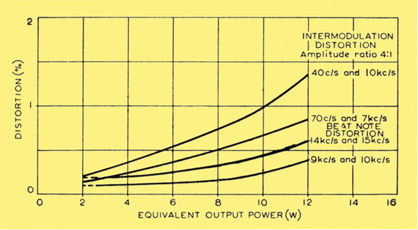
Inter-modulation and 'beat note' distortion characteristics
Sensitivity
The basic sensitivity of the amplifier (that is, the sensitivity at the control grid of the EF86) is 2 mV without feedback and 40 mV with feedback. The sensitivity at the input terminals, thus including the controls, is 600 mV with feedback. The basic sensitivity at the overload point (14 W output) measured with feedback is 50 mV.
Hum and Noise
The level of background noise and hum in the prototype equipment is at least 75dB below the rated output of l0 W.
Phase Shift
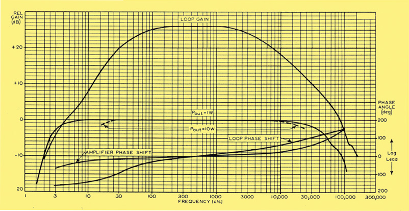
Frequency response, loop-gain and phase-shift characteristics
The phase shift in the amplifier is low. As shown above, the shift is 200 at 20 Hz and at 10 kHz.
Frequency Response
The frequency-response characteristic for an output power of 1 Watt the power-response characteristic for 10 W output power under normal loading conditions are shown in the graph above. It will be seen that the frequency response is level (to within 1 dB) from 5 Hz to 20 kHz and the power response is level from 20 Hz to 15 kHz.
The loop gain characteristic is also plotted in the graph above. This curve shows that 26 dB of feedback are available at 1 kHz.
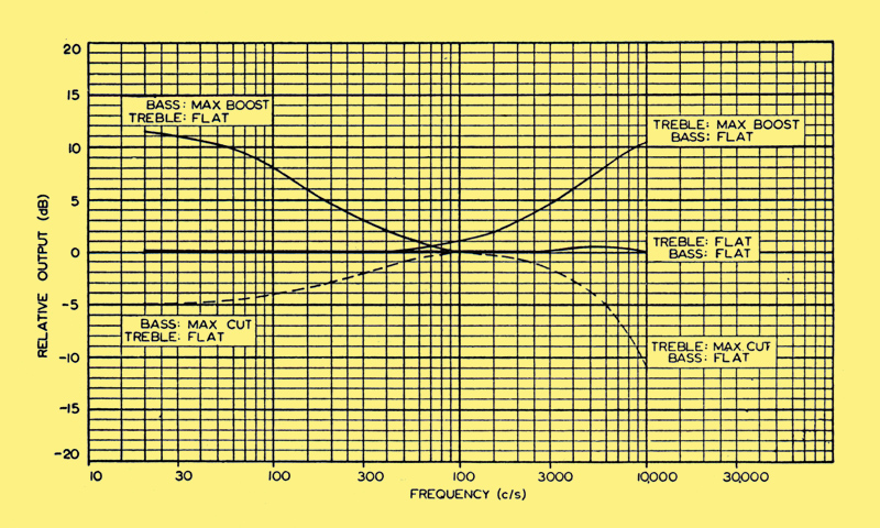
Treble and bass tone-control characteristics
Output Impedance
The output impedance of the amplifier is approximately 0.9 Ω for a 15 Ω load. This gives an adequate damping factor of about 17.
Performance with Normal and Distributed Loading Performance figures are given in the table below comparing the amplifier when a conventional pentode push-pull stage is used with the unit when distributed loading is used.
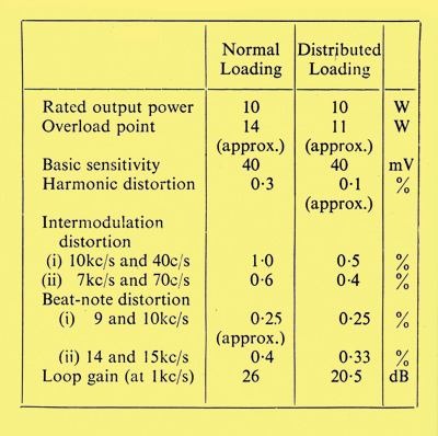
Performance with normal and distributed loading
List of Components
Here is a 1955 advert of a commercially made amplifier to this design.
|