|
The circuits presented in this series have been designed by G A French, specially for the enthusiast who needs only the circuit and essential relevant data. This is circuit 78.
It frequently happens in photographic work and similar pursuits, that the ability to automatically time an operation assumes considerable importance. Various devices can be pressed into service for automatic process timing, and it is possible for these to use quite a number of different operational techniques. However, what is probably the most elegant method of time control employs electronic principles, and a discussion on these forms the introduction to this month's article. The article also describes a suggested circuit for a practical process timer which may be constructed at home by the amateur.
Timing Principles
The normal method of timing a process by electronic means consists of switching the process circuit on or off over a pre-determined period of time. It is usual for the switching operating to be carried out by the contacts of a relay, the length of time this relay remains energised (or de-energised) being governed by the charge or discharge of a capacitor in combination with a resistor. The former may be referred to as the timing capacitor. In conventional arrangements the relay coil is connected in the anode circuit of a valve, whereupon the anode current of this valve can be controlled by applying the potential on one of the plates of the timing capacitor to its grid.
At first sight it would appear that the only requirement of an electronic process timer is merely that the grid potential of the relay valve should be controlled by the timing capacitor potential. In practice, however, this does not represent a complete picture and, for reliable and accurate timing periods, it becomes necessary to pay careful attention to a number of subsidiary design features. The first parts of the timing circuit which require consideration in this context are the relay, and the valve in whose anode circuit it is connected. It is essential that the relay contacts should always operate, at the end of successive timing periods, for exactly the same timing capacitor potential.
Unfortunately, conventional relays cannot be relied upon to operate at the same energising current over a large number of operations. The reasons for this are mainly mechanical: the pressure exerted on the armature by the contact springs may vary with time, the friction opposing the movement of the armature may vary, and so on. In a good electronic timer it therefore becomes necessary to ensure that, at the end of the timing cycle, the change of energising current in the relay coil occurs as rapidly as possible. Ideally, the relay energising current should change instantaneously from an 'on' to an 'off' condition (or vice versa).
In practice, a rapid change in relay energising current may be obtained by using a thyratron as control valve. However, thyratrons raise minor difficulties in their train and do not, in the writer's opinion, represent an ideal choice for a simple home-constructor timing circuit. A good alternative to the thyratron may be given by a hard valve having a very short grid base. Such a valve is capable of passing from the conducting to the non-conducting state for quite a small change in control grid potential.
In order to keep the period of transition in the control valve, and hence the relay, to a relatively low figure, it next becomes necessary to ensure that the potential of the timing capacitor is still changing rapidly at the end of the timing cycle. This condition may be achieved by operating the timing capacitor only over the steeper part of its charge discharge characteristic. Taking arbitrarily chosen figures, a sufficiently rapid rate of change can, in fact, be obtained when the capacitor has charged to approximately 63% (or has discharged to approximately 37%) of the voltage applied to it. The length of time occurring before the capacitor reaches such potentials is, of course, equal to the time constant given by its capacity and the associated resistance. Working to these figures provides the incidental advantage of easing the calculations needed for the timing circuit constants.
This Month's Circuit
Circuit Diagram.
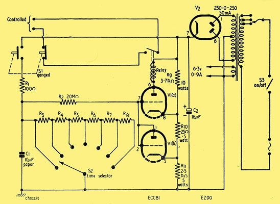
This month's Suggested Circuit takes advantage of the points just detailed. Care has been taken to keep the circuit reasonably uncomplicated and to avoid the use of an excessive number of components. The circuit does not employ any HT voltage stabilisation, as it is felt that such a feature is liable to considerably increase cost without providing any commensurate advantage. Although it is desirable to operate the unit from supply mains of reasonably steady voltage, this is not essential. The circuit has a self-compensatory action (given by the potentiometer network supplying the switching valve), which helps to reduce the effect of heavily fluctuating mains voltages, provided that such fluctuations do not occur during a timing cycle.
The operation of the device is extremely simple. After it has been switched on and allowed to warm up, a timing cycle may be initiated by pressing the spring-loaded switch S1. When depressed, the 'make' contacts of S1 connect the top plate of the timing capacitor C1 to the full HT voltage via the limiting resistor R1. The voltage appearing on the top plate of C1 is applied via R2 to the grid of V1(a), thereby causing this valve to conduct. The relay in the anode circuit of V1(a) energises, and its contacts close. The external, controlled, circuit is not completed yet, however, due to the fact that the 'break' contacts of S1 are open whilst this switch is depressed. As soon as S1 is released, its 'break' contacts complete the external circuit; whilst its 'make' contacts break the HT connection to C1. It is at the instant of releasing S1, therefore, that the timing period commences.
Immediately S1 is released, capacitor C1 starts to discharge into the resistor network, R3 to R8. When the potential on the top plate of C1 drops to approximately 40% of the initial energising voltage it reaches the same value as that on the cathode of V1(a). The potential on C1 still continues to fall rapidly, whereupon it quickly reaches a value sufficiently negative to that on V1(a) cathode for this valve to cut off, whereupon the relay de-energises. The contacts of the relay then break the external circuit and the timing period is finished. C1 continues to discharge into R3 to R8, but this fact is now unimportant, as the operational cycle of the timer has been completed. Whenever S1 is actuated again in order to commence the next timing cycle, C1 will be charged to full HT potential almost immediately.
It will be noted that the timer completes the external circuit over the duration of the timing period. If a particular application necessitates that the timer should break an external circuit over the timing period, the appropriate contacts of the relay and S1 should be altered to have 'break' and 'make' functions respectively.
There are several points of interest in the circuit which have not been fully covered in the brief description of operation just given. The first of these is the reason for fitting the low-value limiting resistor, R1, in series with C1 and the 'make' contacts of S1. R1 is inserted in order to limit the instantaneous current which flows at the moment of operating the switch. If R1 were not in circuit the switch contacts would be liable to burn after a number of operations. The time needed to charge C1 via R1 should normally be negligibly small.
The potentiometer network across the HT supply given by R9, R10 and R11 in series is designed to maintain the cathode of V1(a) at a potential of approximately 40% of the total HT supply. Such a potential is sufficiently close to the 37% (time constant) potential referred to earlier to ensure that the capacitor potential is changing rapidly at the end of the timing cycle. The resistors R9, R10 and R11 need, in practice, have a tolerance of 20% only as any effect on the timing period which divergences from their nominal values may give can be taken up in the network R3 to R8. Assuming a 250 Volt HT line, R9, R10 and R11 draw a standing current of some 40 mA from the HT supply, and maintain the cathode of V1(a) at approximately 100 Volts above chassis. The relay connected in the anode circuit of V1(a) should be capable of operating at an energising current of 6 to 7 mA. A coil resistance around 2,000 Ω would be quite satisfactory.
The valve chosen for V1 is an ECC81 (12AT7), this being a double triode having a short grid base in either triode. It will be noted that only one of the triodes is employed for directly operating the relay, the other being connected as a diode. The purpose of the diode V1(b) is that of preventing excessive grid current and cathode emission in V1(a). When the potential on the top plate of C1 is more positive than that at the junction of R9 and R10, the grid potential of V1(a) is prevented from rising higher than 1 Volt negative with respect to its cathode because of the presence of V1(b). (The cathode of V1(b) is held 1 Volt negative, by means of R10, to V1(a) cathode.) Apart from preventing excessive current in V1(a), the presence of V1(b) in the circuit assists in ensuring a quick and positive transition from the 'on' to the 'off' condition at the end of the timing cycle. When the top plate of C1 is 1 Volt negative to the cathode of V1(a) this valve is 'on' and passes the same anode current as it has done throughout the period; but a further drop of 1 to 1.5 Volts in C1 is enough to make V1(a) 'off'.
Although the values of the resistors R3 to R8 may be worked out approximately, their final values should be considered as being experimental. This is due to the fact, as was just mentioned, that tolerances in R9, R10 and R11 need to be taken up; plus the fact that it is difficult to obtain a close tolerance component for C1. The high-value resistor R2 has a slight effect on timing operation, it tending to increase (by a constant amount) the rate of discharge of C1.
The resistors R3 to R8 may consist of a network of switched resistors, as is shown in the diagram, or of a single potentiometer calibrated in seconds. Due to inaccuracies introduced by track wear the first alternative, that using the switched resistors, is the more preferable. The number of switch positions employed need not, of course, be the same as is shown in the circuit.
The final values of the resistors R3 to R8 may be found in the following simple manner. Let us assume that we wish to select timing periods of 5, 10, 15, 20, 25 and 30 seconds with the aid of S2. It first becomes necessary to find the resistance required for the overall timing period of 30 seconds. We know from the basic circuit design that the resistance required will be approximately that needed to give a time constant of 30 seconds in combination with C1. (The time constant of a CR circuit in seconds is equal to the product of the capacity in μF and the resistance in MΩ) We may start, therefore, by temporarily connecting a 3 MΩ resistor across C1 and measuring the resultant operating cycle. This temporary resistor may then be experimentally altered in value until a period of exactly 30 seconds is obtained. Should the resistance finally obtained be, say, 3.5 MΩ, all the resistors R3 to R8 may be made equal to one sixth of this value. S2 will then select timing periods in 5 second steps up to 30 seconds. As will be appreciated, other timing periods incorporating, if desired, a different number of switch positions may easily be catered for by means of the same technique.
Power Unit
The circuit illustrates a power supply circuit employing a 250-0-250 Volt mains transformer. Although an isolated power supply is desirable in a unit of this type it is by no means essential, and a simple AC/DC arrangement can be employed in its place if desired (Don't do it - Ed). It must be emphasised, however, that if this is done the normal precautions against shock must be observed. It is important, also, to ensure that mains potentials do not appear on the external switching connections. Care is needed here due to the fact that the insulation of relay contacts from their associated metalwork is frequently inadequate for mains voltages.
The Timing Capacitor
Before concluding this article, a few words concerning the timing capacitor C1 would not be out of place. The circuit depicts this capacitor as a 10 μF paper component. A paper capacitor is preferable to an electrolytic component in this position due to the unstable capacity value of the latter. Unfortunately, paper capacitors of the value specified are liable to be somewhat expensive if purchased new, and the constructor is advised to examine the surplus market before spending an excessive amount of money on this component. It may frequently, for instance, be found cheaper to parallel up a number of smaller capacity capacitors obtained from surplus sources than to buy a single new unit of the requisite value.
The writer understands that a particularly suitable condenser is available from H L Smith (Edgware Road). This component has three sections (2.5 + 2.5 + 5 μF) 450 V working, and retails at 10s
|
