|
Correction to give equal amplitudes in both halves of the load.
A push-pull amplifier can be made self-balancing by applying overall push-push negative feedback. The article describes a method of providing this feedback which ensures accurate balance without resort to any close tolerance components.
Although a push-pull amplifier is an item familiar to most of us, it is as well to agree upon what we mean by this term before embarking on a discourse concerned with the finer points of design of such an amplifier. Let us narrow our thought to the simplest push-pull amplifier, shown in Fig. 1.
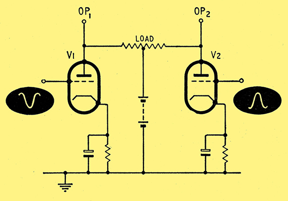
Fig. 1. Basic push-pull amplifier.
We may define such an amplifier as one in which the amplification process is shared equally between the two halves (implying that the two 'halves' of the amplifier are identical). To make our definition complete, we must state that the grids of the two valves are fed with equal signal voltages in anti-phase. We can see that during the period of the input waveform when the anode current of one valve is increasing, the anode current in the opposite valve is decreasing. This feature is responsible for the term push-pull.
The amplifier shown in Fig. 1 is termed balanced, because of its symmetry. If for some reason the amplification is not shared equally between the two valves, we say that the amplifier is unbalanced.
Of the advantages of push-pull operation we may recall, first, that no alternating current of signal frequency flows through the amplifier power supply, thus easing decoupling problems; secondly, that even harmonics unavoidably generated in the amplifier do not appear in the output [1] Radio Engineering, by F E Terman, Sec. 6-11, p.299.. Both these advantages rely upon the amplifier being balanced, particularly if a distributed-load output stage is used [2] Amplifiers and Superlatives. D T N Williamson and P J Walker, Wireless World, Sept. 1952, Vol. 58, p.357.. An amplifier circuit arrangement which is automatically self balancing is therefore desirable. The circuit arrangement of Fig. 1 is unsatisfactory in this respect.
To overcome this disadvantage, it is first necessary to obtain an error voltage which is amplitude and phase dependent upon the degree and direction of unbalance. Following normal servo practice, it is; then possible to reduce the amplitude of the error voltage by the use of negative feedback, so that the amplifier will maintain a high degree of balance even. if the valves and components used in the two 'halves' of the amplifier are unmatched.
The advantages of applying this type of feedback appear to have been first realized, may one say inevitably, by A. D. Blumlein in 1936 [3] British Patent No. 482740, Application Date 4.7.36, A D Blumlein.. In British. Patent No. 482740, Blumlein describes what has become known as a 'long-tailed pair' amplifier. The basic circuit of this form of amplifier is given in Fig. 2.
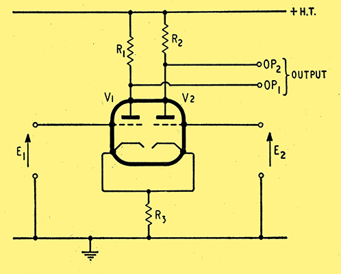
Fig. 2. Basic long-tailed pair amplifier.
The amplifier has two valves, V1 and V2, which have a common cathode resistance or 'long tail', R3, across which is developed the error voltage. The amplifier has a pair of input terminals, to which is applied a push-pull input signal. If the input signal is perfectly balanced about earth, then we know that E1 = -E2. Assuming that V1 and V2 are identical valves, and that the load resistors R1 and R2 are equal, there will be a perfectly balanced output from the amplifier at terminals OP1, OP2,. Under these ideal conditions, with the further proviso that V1 and V2 are linear, there will be no AC potential across R3 because the signal currents flowing in R3 are in anti-phase and of exactly equal amplitude. In fact this resistor serves no useful purpose in this case, and merely increases the required HT line. Provided that a constant anode voltage is maintained, the gain of the amplifier, which may typically be one hundred times, is independent of the value of R3. However, in practice, the above ideal conditions could not be realized for any length of time because of valves and component ageing. This is where the common cathode resistance R3 becomes useful.
To see how this comes about, let us suppose that V1 has a higher mutual conductance than V2. The signal currents flowing in R3 are gmE1, and -gmE2, and in the case we have chosen gmE1, is larger than -gmE2, so that an error voltage is developed across R3 which is in phase with E1. If we now consider the grid-to-cathode drive voltages of V1 and V2, we find that the drive to V1 is reduced by the presence of the error voltage. In contrast the drive to V2 is increased, so that the effective gains of V1 and V2 tend to become equalized, and balance restored. This would also have been the case if we had assumed that V2 had a larger mutual conductance than V1, because the error voltage would then have been in phase with E2. Clearly the above argument applies if the input signal is not perfectly balanced about earth and E1 is not equal to -E2. In fact, a balanced output can be obtained from the circuit of Fig. 2 when the input signal is completely unbalanced, i.e. when E2, for example, is zero. This being so, we may earth V2 grid; and the circuit is now that of a familiar cathode-coupled phase splitter, frequently known as the Schmitt phase splitter [4] Cathode Phase Inversion. O H Schmitt, Journal of Scientific Instruments, March 1938, Vol. 15, p. 100. [5] Phase Splitting in Push-Pull Amplifiers, W T Cocking, Wireless World, April, 1939, Vol. 44, p. 340..
Since the error voltage is the product of the unbalanced anode current and the resistance of R3, it follows that the self-balancing action improves as the resistance of R3 is increased. Analysis of this circuit [6] Push-Pull Input Circuits. W T Cocking, Wireless World, May, 1948, Vol. 54, p. 183. also shows that in order to minimise the unbalance of the output voltage, V1 and V2 should have a large mutual conductance and internal anode resistance. The degree of balance is dependent upon the relative values of R1 and R2. It is common practice to adjust the relative values of R1 and R2 so that an accurately balanced output can be obtained without an unduly large common cathode resistance. In the completely general case, there is a disadvantage associated with this method of achieving accurate balance in the form of increased sensitivity to unwanted signals (e.g. hum) which are present in equal amplitude at each input terminal and are in phase, or if you like, in push-push. The influence of push-push signals is frequently important, and will be considered later.
Long-tailed Pair Refinements
Where an accurate balance is required together with symmetry (R1 = R2) a pentode valve has been used in place of R3 [7] Electro-Encephalograph Amplifier. D L Johnston, Wireless Engineer, Aug/Sept/Oct, 1947, Vol. 24, pp. 231, 271 and 292.. In a circuit of this type the AC value of R3 (pentode anode resistance) may be of the order of a megohm, whereas the DC voltage developed between V1, V2 cathodes and earth need only be of the order of 50-100 Volts. This means that a high impedance is presented to the cathode circuit of V1 and V2 without the large DC voltage drop which would be associated with an ordinary resistor.
The presence of a further valve in the common cathode lead of V1, V2 opens up an important possibility. This is the provision of amplified error-voltage feedback. A method whereby this may be provided [8] Balanced Output Amplifier of Highly Stable and Accurate Balance. Communication from EMI Ltd., Electronic Engineering, June, 1946, Vol. 18, p. 189. is shown in Fig. 3.
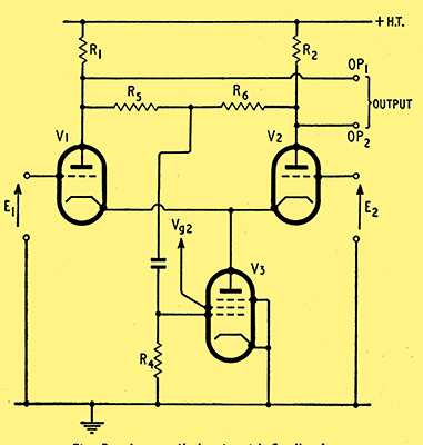
Fig. 3. Long-tailed pair with feedback.
The feedback loop to V3 grid is effective in improving the balance of the output signal. This may be readily seen from the following argument with reference to Fig. 3. Suppose that the signal at V1 anode is for some reason larger than the signal at V2 anode. Assuming that we make R5 equal to R6 a voltage proportional to the unbalance of the output signals will appear at the junction of R5, R6. In the case we have chosen, this error voltage will be in phase with the signal at V1 anode, because this is the larger signal. The error voltage is fed to V3 grid. Any signal fed to V3 grid appears amplified, and with a phase reversal, at each of the two output terminals. Thus the error voltage we feed to V3 grid will produce a signal at V1 anode in antiphase to the original excessively strong signal; and at V2 anode a signal in phase with the original weak signal, tending to reduce the unbalance to zero.
The circuit balance is no longer critically dependent upon the relative values of R1 and R2, but rather upon the relative values of R5 and R6.
Complete Amplifier Balance
By the methods discussed it is thus possible to achieve an accurately balanced signal from an unbalanced input. However, if, as is often the case, a push-pull amplifier contains more than one stage (a push-pull stage employing two valves as in Fig. 1), this is not always of great value, as subsequent stages are likely to introduce unbalance, unless we give them all 'long tails'. When we come to the output stage, where the valves draw a large current, we find that our 'tail' gets very hot! This is undesirable, so let us look now at what happens if we do not provide a large common cathode resistance in the output stage. If the output valves are not matched, we find that it is desirable to compensate for this defect by providing a slightly unbalanced drive.
By adjusting the unbalance of the drive we can choose between zero even harmonics in the output, or zero fundamental component current in the HT line, at one particular signal level [9] Push-Pull Balance. W T Cocking, Wireless World, 1947, Vol. 53, p. 408.; but Nature being as she is, we cannot have both, and either of the above conditions can only be achieved at one signal level!
We want to avoid the necessity of providing a balance control, and we would like our amplifier to remain balanced at all signal levels. It seems logical therefore to provide a push-push feedback loop enclosing the whole amplifier. This idea has been suggested by Offner [10] Push-Pull Resistance Coupled Amplifiers. F Offner, Review of Scientific Instruments, 1937, Vol. 8, p. 20, Figure 4. and is also covered by the Blumlein patent mentioned earlier. However, the idea does not appear to have been fully exploited. Overall feedback may be provided by a simple, but possibly novel, extension of Fig. 3 shown in Fig. 4.
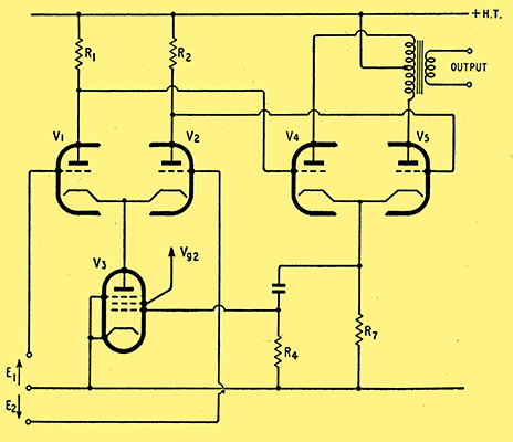
Fig. 4. Amplifier with overall push-push feedback.
Neglecting for the moment even harmonic terms, any unbalance in the amplifier will produce an error voltage of fundamental frequency across the common cathode bias resistor R7 which has an amplitude proportional to the degree of unbalance. The phase of the error voltage depends upon the direction of unbalance. This error voltage is reduced by the feedback loop acting via V3 grid. The important feature is that an excellent balance may be obtained which is not critically dependent on any component values. The degree of valve matching will not now affect the balance of the amplifier, but we shall see that it will influence the harmonic content of the output voltage.
Before discussing this, let us remind ourselves that in a push-pull amplifier even harmonic currents produced by the non-linearity of the output valves cancel by subtraction as far as the load is concerned but are present in the total HT current [1] Radio Engineering, by F E Terman, Sec. 6-11, p.299.. First, let us consider that V4 and V5 are matched, and therefore produce equal even harmonic currents. We know that these even harmonic currents add together to form part of the total HT current. Since this current flows in the common cathode bias resistor R7, a harmonic voltage will be developed across R7. The feedback loop reduces the amplitude of this sum of the even harmonics by a large factor. The push-pull connection prevents even harmonics from appearing in the output, in the usual way.
However, if the output valves are unmatched, it is likely that they will each contribute a different percentage of even harmonic distortion. Although we are able to reduce the sum of the even harmonics, in the limit to zero, We cannot avoid the fact that the difference between the amplitudes of even harmonics produced by each output valve is not zero. We shall therefore have some even harmonic content in the output of the amplifier, in this case.
Pentode Output Stage
So far it has been assumed that triodes have been used in the output stage. When this is the case the common cathode current is one and the same thing as the sum of the two anode currents, provided that the valves do not run into grid current. When V4 and V5 are pentodes, however, the cathode current is made up of the sum of the anode and screen grid currents. Thus by balancing the cathode currents, we have not necessarily ensured that the anode currents, and therefore the load currents, are balanced. With normal receiving valves, however, the unbalance introduced can only be very small, and may be neglected, provided that the valves are not operated to the extremes of their characteristics.
If in a particular application the screen grid current has a detrimental effect, or the valves draw grid current, a circuit of the form shown in Fig. 5 may be substituted.
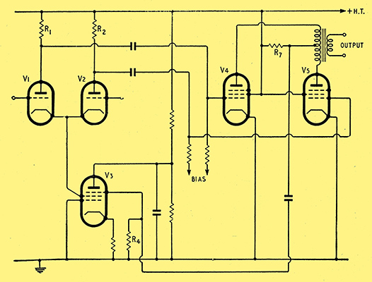
Fig. 5. Alternative feedback circuit.
This arrangement has been simplified to illustrate a principle, rather than provide a working circuit. Naturally we would normally interpose cathode followers between the driver and output valves to supply the grid input power if the valves operate in grid current.
Here the anode currents as such are sampled, and feedback is maintained in the correct sense by changing the connections to V3. The new connections to V3 deserve some further explanation. Let us begin by considering the influence of the suppressor grid potential on the electron stream in the valve. If the suppressor potential is made sufficiently negative, electron flow to the anode ceases. However, the suppressor grid potential cannot influence the cathode current of the valve because it is prevented from influencing the electrostatic field in this region by the screen grid, which we shall assume to be at a constant potential with respect to the cathode. What, then, happens to the electrons we prevented from reaching the anode? The answer is that they alight on the screen grid. We may say therefore that the suppressor potential varies the partition ratio of the anode and screen currents. If the suppressor potential is negative, the greater proportion of current flows to the screen grid, and as we make the suppressor potential more positive, the greater proportion of current flows to the anode. If the total space current remains constant it follows that for a given change of suppressor potential the change in anode current gm(g3-a) is equal and opposite to the change in screen grid current gm(g3-g2). In a valve such as the 6AS6 this gm is approximately 300μA/volt. By connecting the valve in the manner shown in Fig. 5, an error voltage fed to grid 3 produces an in-phase error voltage at the cathodes of V1, V2. This is the condition required for the error voltage feedback to be negative. Alternative circuits which are a combination of Figs. 4 and 5 may prove useful when there are several push-pull stages preceding the output stage. Where this is the case, particular attention must be paid to the coupling time constants, and also to the impedance of the HT supply in determining the stability of the loop.
Influence of Push-Push Signals
It has been briefly mentioned that the influence of push-push signals is important. This is particularly so, for example, in electro-encephalograph amplifiers. It is of interest to consider the extent to which the circuits described respond to these signals. Broadly they may respond in two ways. First, by providing a push-push output signal. Secondly, by converting an unwanted push-push input signal into a push-pull output signal. (There is a further aspect of intermodulation between the push-pull input signal and the push-push input signal but this is beyond the scope of this article.)
Let us consider that the amplifier of Fig. 1 is connected to the receiving end of balanced line subject to electrostatic interference. This is a case where the unwanted signal appears in push-push at the two input terminals. Both V1 and V2 amplify the unwanted signal by equal amounts, so that there will be an amplified push-push interference signal at the output terminals. We may define push-push gain as the ratio push-push output voltage to push-push input voltage. We see that the circuit shown in Fig. 1 has a push-push gain which is equal to its push-pull gain. This is generally undesirable.
However, provided that the circuit is perfectly symmetrical the interference signal will not contribute to the voltage developed between the output terminals, and it is therefore convenient to say that the push-push rejection is infinite. Now let us consider the circuit of Fig. 2; first, in respect of push-push gain. Because we are at present considering a linear system, we are justified in considering the behaviour of the circuit to the unwanted signal, without regard to the wanted signal. To this end, the amplifier may be represented in the simplified form shown in Fig. 6, where E3 represents the unwanted push-push input signal.
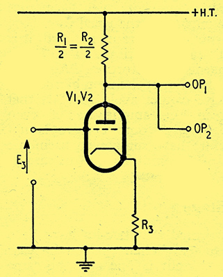
Fig. 6. Long-tailed pair equivalent for push-push signal.
It can now be readily seen that R3 provides negative current feedback in this case. The circuit of Fig. 6 bears a remarkable resemblance to a concertina phase splitter. Indeed we may use this similarity to tell us that if R2/2 = R3, the gain of the amplifier to the unwanted signal will be of the order of 0.9, which is low compared with the amplification of the wanted signal of 100 times. The inclusion of R3, therefore, provides discrimination between push-pull and push-push signals by reducing the amplitude of the push-push output by negative feedback. This is not really surprising, because the balance error voltage we were considering earlier could be regarded as a push-push signal. In Fig. 2, if R1 is equal to R2 and V1 and V2 are identical, then once again the push-push rejection will be infinite. However, if R1 is not equal to R2 there will be a component of the interference signal in the output voltage between terminals OP1 and OP2.

Fig. 7. Circuit of Fig. 3 simplified for push-push operation.
Now let us consider the circuit of Fig. 3, which is redrawn in Fig. 7 to show its operation under push-push drive conditions more clearly. If R4 is made much larger than R5 and R6 in parallel, then as far as push-push signals are concerned, the circuit is that of a cascode amplifier with very nearly 100% feedback. The effect of the additional feedback loop to V3 grid is to further reduce the output of the unwanted signal.
We may conclude that the self balancing systems considered also enhance this aspect of amplifier performance.
To summarise, the balance of a push-pull amplifier can be stabilized to provide equal amplitude signal currents in each half of the load at all signal levels, and at all frequencies handled by the amplifier, by applying overall push-push feedback in the manner shown in Fig. 4. The effect of component tolerances on balance is reduced by this means, and the push-push gain is greatly reduced. The amplitude of signal and harmonic currents flowing in the HT supply is reduced, thus easing decoupling problems; but the amplitude of even harmonics in the output is only zero if the valve curvatures are matched.
Although AC couplings have been shown, there is no reason why DC couplings should not be used, if these are required.
The characteristics of this type of amplifier make it useful as a differential amplifier, that is, an amplifier which responds to the difference between two input signals, irrespective of the individual input levels. It is also useful where a stable and accurate balance is required, or where a large-amplitude unwanted push-push signal (e.g. hum) is present at the input. It is also possible that some benefit may be obtained by applying feedback of this type to a 'Phantom' amplifier [11] Single Amplifier Stereo. Technical Notebook, Wireless World, Feb. 1959, Vol. 65, p. 80. to reduce cross-talk between push-push and push-pull channels at the expense of gain in the push-push channel.
References
- Radio Engineering, by F E Terman, Sec. 6-11, p.299.
- Amplifiers and Superlatives. D T N Williamson and P J Walker, Wireless World, Sept. 1952, Vol. 58, p.357.
- British Patent No. 482740, Application Date 4.7.36, A D Blumlein.
- Cathode Phase Inversion. O H Schmitt, Journal of Scientific Instruments, March 1938, Vol. 15, p. 100.
- Phase Splitting in Push-Pull Amplifiers, W T Cocking, Wireless World, April, 1939, Vol. 44, p. 340.
- Push-Pull Input Circuits. W T Cocking, Wireless World, May, 1948, Vol. 54, p. 183.
- Electro-Encephalograph Amplifier. D L Johnston, Wireless Engineer, Aug/Sept/Oct, 1947, Vol. 24, pp. 231, 271 and 292.
- Balanced Output Amplifier of Highly Stable and Accurate Balance. Communication from EMI Ltd., Electronic Engineering, June, 1946, Vol. 18, p. 189.
- Push-Pull Balance. W T Cocking, Wireless World, 1947, Vol. 53, p. 408.
- Push-Pull Resistance Coupled Amplifiers. F Offner, Review of Scientific Instruments, 1937, Vol. 8, p. 20, Figure 4.
- Single Amplifier Stereo. Technical Notebook, Wireless World, Feb. 1959, Vol. 65, p. 80.
* D R Birt - Mullard Research Laboratories.
|