|
This article gives fall constructional details of an inexpensive amplifier which is capable of a very high performance level.
Despite the fact that present-day audio amplifying and reproducing equipment tends to be centred on complex and relatively costly amplifiers there is a very considerable demand amongst constructors for amplifiers which, whilst being capable of offering a high performance level, are smaller and less expensive. The Cooper-Smith 'Bantam' falls into this category, and it has been designed to give a quality of reproduction which is considerably in advance of that provided by standard radios and radiograms. The 'Bantam' possesses all the features normally found in much more complex equipment: it has continuously variable bass and treble controls, it contains its own mains power unit, it can provide heater and HT power for ancillary equipment such as FM tuner units and the like, and it is capable of driving speakers at either 15Ω or 3.75Ω impedance. The output stage is single-ended, the output valve specified being rated at a high power figure. This valve works into an output transformer having a generously heavy core, negative feedback from its secondary being applied to the stage preceding the output valve.
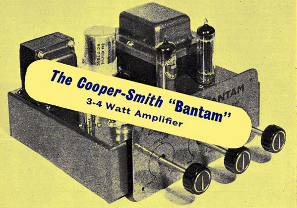
As may be seen from the photograph at the head of this article, the completed amplifier presents a very neat and professional appearance. A separate escutcheon, also shown in the photograph, enables the amplifier to be mounted in a cabinet, if desired, the control spindles protruding through the escutcheon.
Technical features for the 'Bantam' are as follows:
- Power Output: 3-4 Watts
- Frequency Response: 40 - 25,000 Hz ±1dB at 1 Watt (tone controls flat).
- Tone Controls: Bass and treble cut and boost, continuously variable.
- Output Impedances: 3.75Ω and 15Ω.
- Input Sensitivity: 60mV for 3 Watts output.
- Valves: ECF80, EL84 (or 6BQ5), EZ81.
- Spare Power: 250V at 45mA, 6.3V at 2A.
- Weight: 8.75lb.
- Size: 8 x 6.5 x 4.5in.
The Circuit

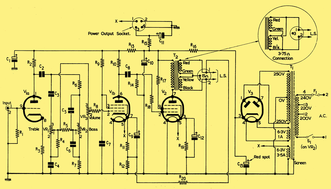
Fig. 1. The theoretical circuit of the Cooper-Smith Bantam. The identification numbers on potentiometers and sockets apply to the similarly numbered tags in Fig. 2
The circuit of the Bantam appears in Fig. 1. The input signal is applied to the grid of V1(a), this being the triode section of an ECF8O. V1(a) functions as a triode voltage amplifier and compensates for the loss of signal voltage occurring in the subsequent tone control circuit. A small degree of current negative feedback is applied to the input stage by means of the un-bypassed cathode resistor R3.
The signal on the anode of V1(a) is fed to the tone control circuit around potentiometers VR1 and VR2. This circuit is one which has been well-proven in practice, and was successfully incorporated in the Cooper-Smith Mark II Control Unit. The output from the tone control circuit is applied to the upper terminal of VR3, the volume control; the signal level tapped off by the slider of this control being fed, via the grid-stopper R8, to the pentode section, V1(b) of the ECF80.
The pentode also functions as a voltage amplifier, the amplified signal appearing across its anode load, R10. Due to the choice of valve and operating conditions, V1(b) anode has a relatively low impedance to chassis. The anode of V1(b), working at this relatively low impedance, then drives the grid of the output valve, V2, via the grid stopper, R18.
The output valve functions in conventional manner, feeding into the speaker transformer T2, the secondary of which connects to the loudspeaker output socket. In the main circuit diagram the two secondary windings are connected in series, thereby offering an output impedance of 15Ω. In the 'inset', the secondary windings are connected in parallel, offering an output impedance of 3.75Ω.
Negative feedback is obtained from the secondary of the speaker transformer via R20. This resistor, with R12, forms a fixed potentiometer which causes a proportion of the secondary output voltage to be injected into the cathode of V1(b). For 15Ω output operation R20 has a value of 22kΩ. For 3.75Ω output operation (in which half the signal voltage given for 15Ω operation is available across the secondary of T2) R20 has a value of 10kΩ.
HT power in the 'Bantam' is obtained by means of a mains transformer having a full wave HT secondary, rectification being provided by V3. V3 cathode connects into the filter components C13, R16, and C10, the output valve, V3, obtaining its HT supply from the smoothed voltage appearing across the latter capacitor. Further smoothing is provided by R13 and C1, the voltage across C1 being employed for V1(a) and V1(b).
The power supply has been designed to provide an HT output of 250 Volts at a maximum current of 100 mA. The amplifier current requirement is 55 mA only, with the result that an HT voltage of 250, with a maximum current of 45 mA, becomes available for ancillary equipment such as radio tuners, etc. Such equipment may obtain HT and heater power from the power output socket shown in Fig. 1. Since individual requirements may vary, a value for the HT series resistor, R15, has not been specified; this being chosen to suit the particular needs of the equipment envisaged. If, to take an example, the ancillary equipment were to require an HT supply of 200 Volts at 40 mA, then R15 would be required to drop 50 Volts (from the 250 volts available in the amplifier) at this current. From Ohms Law R=E/I the required value for R15 under these circumstances would be 50/0.04 = 1,250Ω. Should the amplifier be purchased in kit form, either the value for R15, or the voltage and current requirements of the associated equipment, should be specified.
A 6.3 V heater supply is also available at the power output socket, this being obtained from the same heater winding of the mains transformer which feeds the heaters of V1(a), V1(b), and V2. The heater current available at the socket is 2A.
Construction
Construction of the Cooper-Smith 'Bantam' is a relatively simple procedure. The photographs accompanying this article show very clearly the clean and neat layout employed, and they will be of assistance during the process of mounting components and wiring up. A layout and wiring diagram is given in Fig. 2, this showing the position of all components and connections. It will be noted, in Fig. 2, that individual tags on potentiometers, valve-holders, sockets and the mains voltage selector panel are numbered. These numbers correspond to those appearing in the circuit diagram of Fig. 1. Also shown numbered are the tags on the two 12-way tag-strips. All these tags are referred to by their numbers in the step-by-step instructions which follow. The rear apron of the chassis in Fig. 2 is shown opened out in order that connections made to the components mounted on it may be illustrated more clearly.
Step-by-Step Instructions
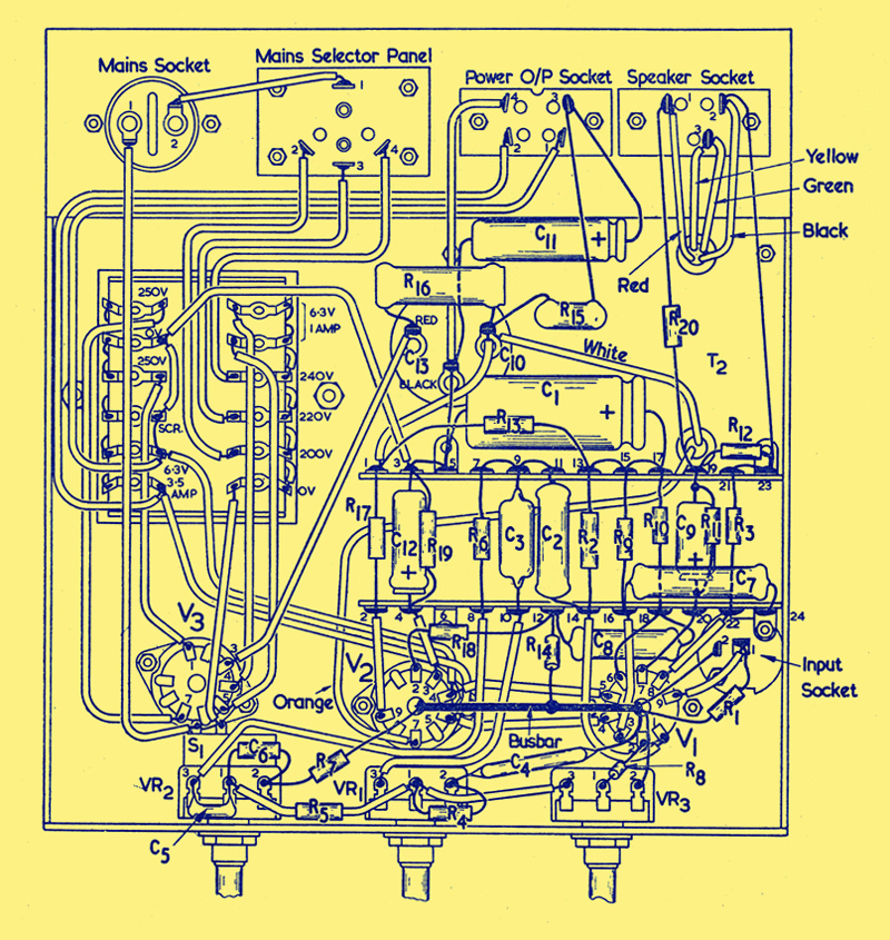
Fig. 2. Layout and wiring diagram. The rear apron of the chassis is laid flat to show the connections to the rear sockets and the mains selector panel more clearly.
Construction proceeds as follows:
- Fit the mains socket, mains selector panel, power output socket and speaker socket to the rear apron. All these are fitted from the inside except for the mains socket.
- Fit the mains transformer T1, ensuring that its tags take up the position shown in Fig. 2. Also, fit the speaker transformer T2, bringing its leads out as shown in Fig. 2. It is necessary for the lower right-hand nut (adjacent to the tag - fitted later -numbered 23 in Fig. 2) to make good contact to chassis. Ensure good contact by scraping, or cleaning, the underside of the chassis before this nut is fitted.
- Fit the dual capacitor C10, C13, ensuring that the tag marked red is nearest the mains transformer T1. Make certain of good chassis contact to the capacitor clip by scraping the underside of the chassis at the points where the mounting nuts tighten down.
- Fit the input socket, ensuring correct orientation (its earthy tag, 2, should take up the position shown in Fig. 2). Again, scrape the chassis to ensure good contact to its mounting nuts.
- Fit the valve-holders, ensuring correct orientation. Note that V1 valve-holder has a skirt (see photographs) and is mounted above the chassis, and that V2 and V3 valve-holders are mounted below. Scrape the chassis to ensure good contact to the securing nuts for V1 valve-holder.
- Fit a 6BA nut and bolt (again scraping the underside of the chassis to give good contact) to the hole hear V2. (R18 - fitted later - is above this hole in Fig. 2.) Mount the two 12-way tags-trips as shown in Fig. 2. The lower tag-strip is mounted over the 6BA bolt just fitted, and over the outside bolt securing the input socket. The upper tag-strip is mounted over the lower right hand bolt securing the speaker transformer (referred to in step 2) and the lower bolt securing the dual capacitor C10, C13. Both tag-strips are mounted over the nuts which have previously been tightened, and are secured by fitting additional nuts.
- Fit the three potentiometers VR1, 2 and 3, to the front panel as shown in Fig. 2 (noting the locating holes in the chassis).
Wiring Up
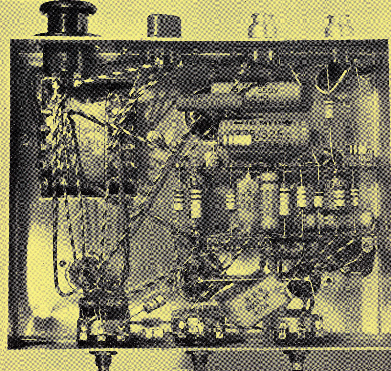
Under-chassis view of the 'Bantam'. This view, which demonstrates the clean wiring layout, may be compared with Fig. 2.
Wiring up now commences. In order that all connections may be made to each individual tag before they are soldered to that tag, soldering should only be carried out where stated.
- Using twisted wiring, connect in parallel pins 4 and 5 of V1, pins 4 and 5 of V2, the 6.3 V 3.5 A tags on T1, and tags 1 and 2 on the power output socket. Solder all these joints except the 6.3 V 3.5 A tag on T1 adjacent to the 'SCR' tag. Also using twisted wiring, connect in parallel, and solder, pins 4 and 5 of V3 and the 6.3 V 1 A tags on T1. (Fig. 2 shows this wiring step with untwisted wire for ease of circuit tracing.)
- Carefully following Fig. 2, connect the 6.3 V 3.5 A tag on T1 adjacent to the 'SCR' tag to that tag, carrying on to the 0 V tag (HT secondary) on T1, and to tag 3 of the tag-strips. Solder all joints except tag 3.
- Carefully following Fig. 2, connect 0 V tag (mains primary) on T1, to one tag of switch S1 and solder. Connect 200 V tag on T1 to tag 2 of mains selector panel and solder. Connect 220 V tag on T1 to tag 3 of mains selector panel and solder. Connect 240 V tag on T1 to tag 4 of mains selector panel and solder. Connect the two 250 V tags on T1 to pins 1 and 7 of V3 and solder.
- The speaker transformer, T2, is next connected into circuit. Connect its orange lead (following route in Fig. 2) to pin 7 of V2 and solder. Connect its white lead (following route in Fig. 2) to C10.
- For 15Ω output only. Connect red lead of T2 to tag 1 of speaker socket. Connect black lead of T2 to tag 2 on speaker socket. Connect yellow and green leads to tag 3 on speaker socket, soldering at tag 3. These connections are shown in Fig. 2.
- For 3.75Ω output only. Connect red and yellow leads of T2 to tag 1 on speaker socket. Connect green and black leads of T2 to tag 2 on speaker socket. These connections are not shown in Fig. 2.
- Tag-strip connections come next. Connect R17 (100Ω) between tags 1 and 2.
- Connect R19 (150Ω) and C12 (50μF, 25 W.V.) between tags 3 and 4, observing correct polarity in C12. Join tags 3 and 5. Solder tag 3.
- Connect C1 (16μF, 275 W.V.) between tags 5 and 17, observing correct polarity.
- Connect R6 (68kΩ) between tags 7 and 8.
- Connect C3 (560pF) between tags 9 and 10.
- Connect C2 (0.02μF) between tags 11 and 14. Join, and solder, tags 7, 9 and 11.
- Connect R2 (100kΩ 0.5W - as opposed to the 0.25 W R10) between tags 13 and 14.
- Connect R9 (470kΩ) between tags 15 and 16.
- Connect R10 (100kΩ) between tags 17 and 18. Join tags 13, 15 and 17, soldering at 15 and 17.
- Connect C9 (50μF, 12 W.V.) and R11 (1.8kΩ) between tags 19 and 20, observing correct polarity of C9.
- Connect R3 (l.2kΩ) between tags 21 and 22.
- Connect R12 (100Ω) between tags 19 and 23. Join tags 21 and 23, soldering at 21.
- Connect R13 (22kΩ 0.5 W - as opposed to the 0.25 W R20 when 15Ω output is used) between tags 1 and 13, soldering at 13.
- Connect C8 (0.05μF) between tags 12 and 18.
- Connect C7 (0.1&mu:F) between tags 16 and 24, soldering at 24.
- The rest of the wiring is now continued. Following the route shown in Fig. 2, connect pin 3 of V3 to C13, soldering at pin 3.
- Following Fig. 2, connect and solder the remaining tag of switch S1 to tag 1 of the mains socket.
- Connect and solder tag 2 of the mains socket to tag 1 of the mains selector panel.
- Following Fig. 2, identify the negative (black) tag of C10, C13. All the following connections involve this tag. Connect the negative tag of C10, C13 to tag 5 on the tag-strips, soldering at tag 5. Connect the negative tag of C10, C13 to tag 4 on the power output socket, soldering at tag 4. Connect C11 (8μF, 350 W.V.) between the negative tag of C10, C13 and tag 3 on the power output socket, observing correct polarity. Solder at negative tag of C10, C13.
- Following Fig. 2, connect C10 to tag l on the tag-strips, soldering at tag 1.
- Following Fig. 2, connect R16 (470Ω) between C10 and C13, soldering at C13.
- Following Fig. 2, connect and solder R15 (value according to requirements - see above) between C10 and tag 3 on the power output socket.
- Connect and solder R20 (22kΩ for 15Ω output, 10kΩ 0.25 Watt, as opposed to the 0.25 Watt R18, for 3.75Ω output) between tag 19 of the tag-strips and tag 1 on speaker socket.
- Join, and solder, tag 23 of the tag-strips to tag 2 on speaker socket.
- Join tag 1 on input socket to pin 9 of V1. Solder at pin 9.
- Bend the supplied thick piece of wire at right angles, 0.75 inch in from each end, and solder to centre spigots of V1 and V2 to form a busbar between them. (The bent ends enter the spigots, and the the busbar is shown in heavy line in Fig. 2.) All connections made to the busbar which follow are soldered at the busbar.
- Join and solder pin 2 on the input socket to the busbar.
- Connect and solder R1 (1MΩ 0.125 W - as opposed to the 0.25 W R14) between tag 1 of the input socket and the busbar.
- Join and solder pin 8 of V1 and tag 22 of the tagstrips.
- Join and solder pin 7 of V1 and tag 20 of the tag-strips. Use sleeving (omitted from Fig. 2 for clarity).
- Join and solder pin 6 of V1 and tag 18 of the tag-strips. Use sleeving (omitted from Fig. 2 for clarity).
- Join and solder pin 3 of V1 and tag 16 of the tag-strips.
- Join and solder pin 1 of V1 and tag 14 of the tag-strips.
- Connect and solder R8 (1kΩ) between pin 2 of V1 and tag l of VR3.
- Connect R18 (10kΩ) between pin 2 of V2 and tag 12 of the tag-strips. Solder at pin 2.
- Join and solder pin 3 of V2 and tag 4 of the tag-strips.
- Join and solder pin 9 of V2 and tag 2 of the tag-strips.
- Join tag 3 of VR2 to tag 8 of the tag-strips, and solder at tag 8. Follow route shown in Fig. 2.
- Join and solder tag 3 of VR1 to tag 10 of the tag-strips. Follow route shown in Fig. 2.
- Connect and solder R14 (1MΩ) between tag 12 of the tag-strips and the busbar.
- Connect C5 (2,000pF) between tags 1 and 3 of VR2. Solder at tag 3.
- Connect C6 (0.02μF) between tags 1 and 2 of VR2.
- Connect and solder R7 (6.8kΩ) between tag 2 of VR2 and the busbar.
- Connect R5 (39kΩ) between tag 1 of VR2 and tag 1 of VR1. Solder at tag 1 of VR2.
- Join tag 1 of VR1 and tag 3 of VR3. Solder at tag 3.
- Connect R4 (47kΩ) between tags 1 and 2 of VR1. Solder at tag 1.
- Connect and solder C4 (8,000pF) between tag 2 of VR1 and the busbar.
- Join and solder tag 2 of VR3 to busbar.
- Fit valves and knobs.
Operation
The Cooper-Smith 'Bantam' is now complete and ready for operation. The voltage selector panel should be set to the mains voltage with which the amplifier is to be used. The main input fuse (rating 2 A) is housed in the bridging plug of the panel. The speaker should be connected to pins 1 and 2 of the speaker socket (tag 3 of this socket, used for the 15Ω output impedance connection, is an anchoring tag only).
The input sensitivity of the amplifier is 60 mV for 3 Watts output, and care should be taken to avoid applying excessive inputs. If the associated radio tuner or pick-up provides an output considerably in excess of 60 mV it will be necessary for this to be attenuated before coupling to the amplifier. Suitable attenuation will normally be given by providing a pre-set potentiometer before the input socket, this being adjusted until a smooth control is provided by VR3. As a rough guide to the correct setting of such a potentiometer, the amplifier should begin to overload when VR3 is some three-quarters advanced.
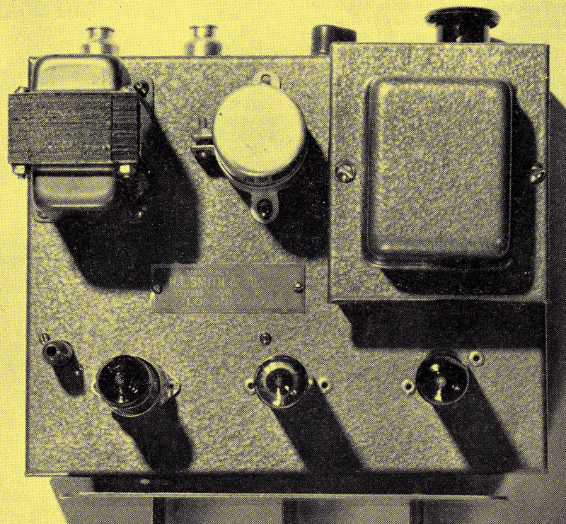
Top view of the chassis, illustrating its neat appearance. The rectifier, V3, is at the mains transformer end of the chassis, whilst V2 is in the centre.
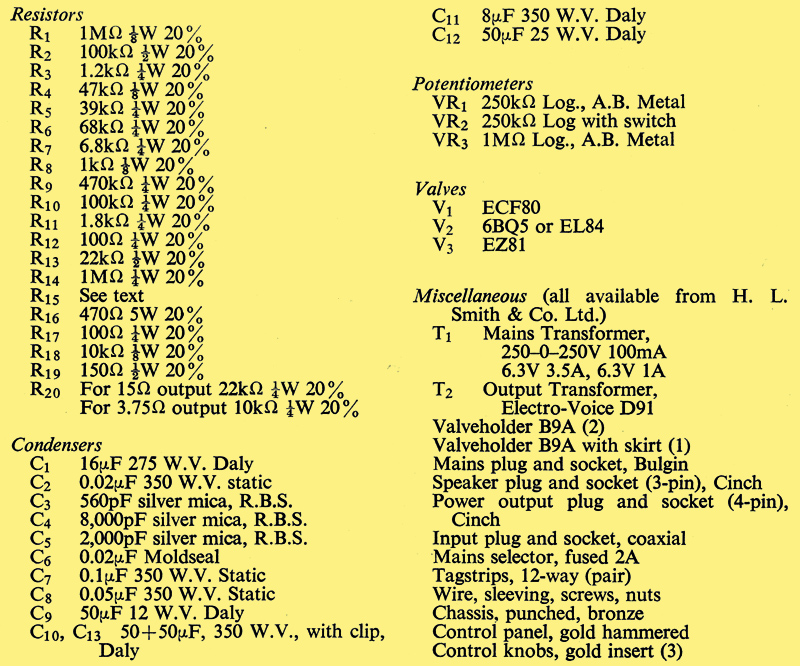
The Components List
|