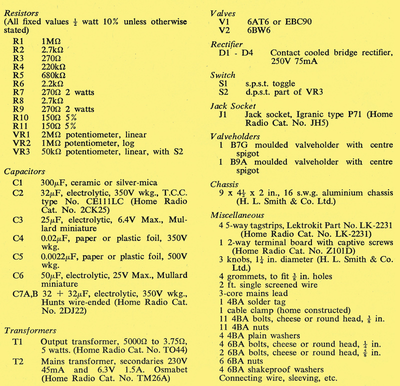
|
Designed for ease of assembly, this amplifier employs a reliable circuit which is simple for the beginner to follow and understand. Treble and bass tone controls are provided, and an unusual feature is the inclusion of a switched negative feedback loop. To assist in construction, the drilling and wiring diagrams are published in the special supplement.
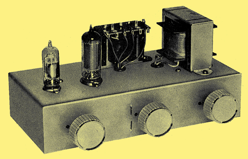
The completed amplifier
An amplifier is always an attractive item of equipment as it not only lends itself to domestic entertainment requirements but can also be used for experimental or servicing work in the workshop. Although designed primarily for entertainment purposes, the 'Neophyte' amplifier offers many more serious functions as well. An interesting departure from normal practice is the inclusion of a switch in the negative feedback loop. When this switch is opened, the amplifier offers increased gain without, of course, the benefits of distortion reduction which are imparted by feedback. With the negative feedback switch closed, the amplifier is mainly intended for monaural reproduction from a crystal gramophone pick-up. It may also accept inputs of about the same amplitude from radio tuner units and other audio signal sources.
The Circuit
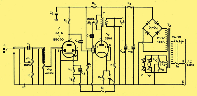
The full circuit
The circuit of the amplifier appears in the diagram above. Signal input is applied to jack socket J1 and then passes to the bass tone control network given by C1, VR1 and R1. The bass control network is followed by volume control VR2, the slider of which couples to the grid of V1 triode. All the input circuitry is at high impedance, and is suitable for the direct connection of a crystal pick-up. The interconnecting wires inside the amplifier are screened in order to suppress mains hum.
V1 (6AT6 or EBC90) is a double diode triode, the two diodes of which are unused and are connected to chassis. The amplified signal at the anode of V1 couples to the control grid of V2 by way of C4 and grid resistor R5. V2 is a beam tetrode type 6BW6. This is the B9A version of the octal 6V6, the latter being a valve which has acquired well-earned popularity over a considerable period because of its ability to provide a low-distortion audio signal in non-critical single-valve output stages.
The anode signal from the 6BW6 is applied to the primary of output transformer T1, this having a ratio suitable for coupling to a 3Ω loudspeaker. The treble tone control, VR3, is connected across the primary of T1 and its function is to apply a selected proportion of the anode signal to C5, and thence to the cathode of V1. This represents a negative feedback loop, the value of C5 being such that the signal level fed back increases with frequency. Thus, the circuit causes less amplification to be given to the higher audio frequencies, and provides a variable control of treble attenuation.
Another negative feedback connection is taken from the secondary of T1 and applied, via R8 and S1, to the cathode of V1. The addition of S1 is a novel feature in an amplifier of this nature, and it increases the versatility of the design at the cost of only one component, this being the switch itself. If, for any reason, a higher degree of gain is required than would be available with feedback applied, S1 is opened. The amplifier then offers increased gain, but without the reduction in distortion imparted by the feedback. The tone control offered by VR3 is still available when S1 is opened.
The power supply employs a mains transformer offering complete isolation from the mains. An extremely economical combination is provided by the use of a contact-cooled bridge rectifier (D1 to D4) in conjunction with a transformer having a single untapped 230 Volt HT secondary. The transformer employed does not have a centre-tapped 6.3 Volt heater winding and it would be normal practice to have one side of the heater supply circuit connected to chassis. However, due to the facts that V1 grid is at high impedance and that the circuit may be built by newcomers to the hobby, it was decided to provide an effective centre-tap into the heater supply by means of the two equal-value resistors, R10 and R11, their junction being connected to chassis. This eliminates a possible cause of hum before construction is even commenced and, for the cost of two resistors, the extra precaution was considered worthwhile. In the amplifier, as built, the connections to the heaters of V1 and V2 are carried out with twisted wiring.
Components
The components required for the amplifier are specified in the accompanying Components List, and a few words are required concerning some of these. It will be noted that the electrolytic capacitors have their manufacture and type, or a retail catalogue number, quoted. The reader is strongly advised to obtain the types specified, as alternative components of the same capacitance and rating may prove to be bulkier in size. This point applies in particular to C7a+b, which has to fit between two tag-strips. (modern components will be smaller and so this should not be a problem - ed.)
The output transformer quoted is a type intended for operation at 5 Watts, as is available from the 6BW6 in the circuit employed here, and it would be unwise to attempt to use a smaller component. The transformer is listed in the Home Radio range of economically priced output transformers, with manufacturers as available. In consequence, the tag positioning of the specific transformer obtained by the constructor may vary from that in the transformer used for the prototype. The constructor should initially satisfy himself concerning the tags to which the primary and secondary windings connect: if no other indication is provided, it will usually be found that the secondary leads from the winding to the tags consist of the enamelled wire employed in the winding itself, whilst the primary leads from the winding are PVC covered. Also, the secondary will have a very low resistance, whilst the primary will have a resistance of the order of 300Ω.
The mains transformer should have an indication as to which of its leads connect to the primary (or transformer input) and which to the 230 Volt HT secondary. It is usual practice for the HT secondary leads to be covered with red insulation. The transformer used in the prototype had no mains primary tappings. Should such tappings be provided, the constructor should select the tap appropriate to the local mains voltage, tape up the remaining primary leads separately and tuck them out of the way in any convenient manner so that there is no risk of their short-circuiting to chassis or to any other component. The 6.3 Volt heater winding lead-outs will consist of the enamelled copper wire with which the heater secondary is wound.
The dimensions given in the chassis drilling diagram apply only to the two transformers specified. The tag-strips quoted are Lektrokit types, these being 5-way with the centre-tag earthed (i.e. the centre tag is used also for mounting the tag-strip to the chassis). The four non-earthy tags have anchoring points at the upper and lower ends, and this fact is of assistance during wiring. The tag-strips are not sold singly, and it is necessary to purchase them in packets of twelve. Thus, some tag-strips will be left over for other projects after the amplifier has been built.
The three controls, VR1, VR2 and VR3/S2, will be supplied with spindles which are probably too long for most requirements. The spindles should be cut to the desired final length with a hacksaw before fitting the controls to the chassis.
A further point is concerned with the fact that a short length of single screened wire is required for connections inside the amplifier. Television aerial coaxial cable could be used here, but it is rather bulky for the present purpose. A neater job will result if the constructor uses the much thinner type of screened flexible cable which is intended for audio wiring.
The mains lead must be a 3-core type of suitable length, and it should be terminated in a 3-way mains plug with earth connection. It is preferable to use a mains lead having a PVC outer sheath rather than one with a woven fabric covering, since the former is easier to handle. As is described later, a small cable clamp has to be made up to anchor the mains lead inside the chassis.
Preparing the Chassis
Drilling dimensions for the chassis are given on the first sheet of the supplement. The chassis material is 16 SWG aluminium.
The upper drawing shows the view looking down on the top of the chassis. The 0.625 in. and 0.75 in. holes are for the B7G valve-holder (V1) and B9A valve-holder (V2) respectively. When these holes have been cut out, use the valve-holders themselves as templates for marking out the two 6 BA clear mounting holes (indicated as 'A') required for each valve-holder.
The three 0.375 in. holes are intended for rubber or PVC grommets. The drawing indicates, also, the mounting holes which will be used by T1 and T2. The centre diagram shows the front apron as viewed when looking at the front of the chassis. Three holes for the controls are required here, as indicated. The 0.125 in. holes alongside the bush-mounting holes are intended for the locating lugs of these controls.
The lower diagram illustrates the rear apron as seen when observing the chassis from the rear. Two sets of holes on the rear apron have to be marked out with the aid of the components themselves. First, take up the rectifier obtained for D1-D4, centralise it on the line between X and X1, then mark out the two 6BA clear holes required for mounting along the central horizontal line. Secondly, initially drill the two 0.4375 in. holes at the centre of the rear apron. Then, take up the 2-way terminal board, hold it against the apron in its final position and, ensuring that its internal tags and screws do not short-circuit against the edges of the two 0.4375 in. holes, mark out its 4BA clear mounting holes. The 0.375 in. hole in the rear apron is for a grommet, and the remaining two holes for the jack socket and switch S1.
When drilling is complete, clean up the chassis and remove all burrs, etc. Ensure that the locating lugs of the three front panel controls fit comfortably into their 0.125 in. holes. Check, in particular, that there are no burrs or other projections on the holes for D1-D4 which would prevent this component from making good thermal contact to the chassis. No components are mounted at this stage.
Wiring and Assembly
The next process consists of wiring and assembly, and the constructor should work from the wiring and layout diagram on the centre sheets of the supplement. Here, the front and rear aprons are shown 'opened-out' for convenience of illustration. Note that the tags of the tag-strips are numbered 1 to 20 to facilitate identification. The upper anchoring points for the tags (i.e. those furthest away from the chassis) are assumed, in the diagram, to project on the opposite side of the Paxolin strip to the mounting lug. (In practice, both anchoring points are on the same side of the strip.)
In the assembly steps which will next be given, soldering at a particular tag should only be carried out when stated. This avoids the rather undesirable practice of adding a lead to a tag which is already soldered up. All soldered connections must be made with the aid of resin-cored solder, such as is manufactured by Multicore Solders Ltd. On no account attempt to use a paste or liquid flux.
- Mount tag-strips 1-5, 6-10 and 16-20 with 4 BA nuts and bolts, so that they take up the positions shown in the wiring digram. Be careful to ensure correct orientation.
- Mount V1 and V2 valve-holders with 6 BA nuts and bolts, orientating these so that pins 3 and 4 of V1 valve-holder, and pins 4 and 5 of V2 valve-holder, are nearest the front apron.
- Fit all four grommets to the top surface and rear apron.
- Take up the mains lead and strip back its outer sheath for 3.5 in. Pass the stripped end through the rear hole intended for it. Fabricate a simple cable clamp from an oddment of metal (quite an adequate clamp may be made by suitably bending a centre lug taken from one of the unused tag-strips) and clamp the cable as illustrated in the diagram, using a 4 BA nut and bolt. If there is any risk of the cable sheath chafing against the clamp, wrap PVC insulating tape around it.
- Fit a 4 BA chassis tag, as shown, and solder the earth mains wire (green and yellow striped with the new mains lead coding system) to this.
- Mount the mains transformer, T2, with 4 BA nuts and bolts, fitting plain washers under the bolt heads. The four secondary lead-outs pass through the grommet adjacent to tag-strip 1-5, and the primary lead-outs pass through the grommet over which the mains lead passes. If the primary has voltage taps, deal with these as described earlier.
- Shortening as necessary, connect the 6.3 Volt secondary leads from T2 to tag 1 (lower) and tag 5 (lower). Take care to ensure that the enamel on the transformer leads has been removed and that the copper underneath is properly tinned. Solder at tag 1 (lower) and tag.5 (lower). It does not matter which secondary lead connects to which tag.
- Using two wires twisted together, connect pins 3 and 4 of V1 to pins 4 and 5 of V2. Again using two wires twisted together, connect pins 4 and 5 of V2 to tag 1 (upper) and tag 5 (upper). Solder the four connections made at V1 and V2.
- Connect R10 (150Ω) between tag 1 (upper) and tag 3 (upper). Connect R11 (150Ω) between tag 5 (upper) and tag 3 (upper). Solder at tags 1, 3 and 5 (all upper).
- Fit VR3/S2 to the front apron. With an ohm-meter or any simple continuity tester identify the tags of the switch sections which correspond to the switch poles, as the tag positions with some switches may differ from those shown in the diagram.
- Shortening as necessary, connect the line and neutral wires from the mains lead to one side each of the two switch poles. (With the new coding system, brown is live and blue is neutral). Shortening as necessary, connect the two primary leads of the mains transformer to the other sides of the two switch poles. It does not matter which primary lead connects to which switch pole. Solder all four connections at S2.
- Mount the rectifier D1 to D4, with its flat. side against the chassis inside surface, using 0.625 in. 6 BA bolts and fitting shake-proof washers both under the bolt heads and under the nuts. The rectifier lugs should take up the positions shown in the diagram.
- Shortening as necessary, connect the 230 Volt HT secondary leads from T2 to the two AC tags (marked with a sine wave) of the rectifier. Solder these two connections. It may be found convenient to pull a few inches of the mains lead inside the chassis and keep it out of the way whilst soldering the tag adjacent to it. It does not matter which secondary lead connects to which rectifier tag.
- Connect a wire between the negative tag (marked -) of the rectifier and tag 8 (upper). Connect a wire between the positive tag (marked +) of the rectifier and tag 10 (lower). Solder all these four connections.
- Connect R6 (2.2 kΩ) between tag 9 (upper) and tag 6 (upper). Connect R9 (270Ω 2 Watts) between tag 10 (upper) and tag 6 (upper).
- Connect R4 (220 kΩ) between pin 7 of V1 and tag 20 (lower). Connect a wire between tag 20 (lower) and tag 9 (lower). Solder at tag 20 (lower) and tag 9 (lower).
- Connect C4 (0.02μF) between pin 7 of V1 and pin 2 of V2, so that it takes up the position shown in the wiring diagram. Similarly connect R5 (680 kΩ) between pin 2 of V2 and V2 centre spigot. Connect a wire between V2 centre spigot and tag 18 (upper). Solder at pin 7 of V1, pin 2 of V2 and V2 centre spigot.
- In this step and step 20, the components C3, C5, R2 and R3 are wired into circuit. For illustration these are shown further away from tag-strip 16-20 than they need be. The constructor should wire these components so that they are neatly parallel with the strip and close to it. Connect C5 (0.0022μF) between tag 17 (upper) and tag 19 (upper). Connect R3 (270Ω 0.5 Watt) between tag 18 (upper) and tag 19 (upper). Connect a wire between V1 centre spigot and tag 18 (upper). Solder at tag 17 (upper) and tag 18 (upper).
- Connect a wire between tag 17 (lower) and the centre tag of VR3, the wire following the route shown in the diagram. Solder both these connections.
- Connect R2 (2.7 kΩ) between tag 19 (lower) and tag 16 (lower). Connect C3 (25μF) between tag 19 (lower) and tag 16 (lower) with its positive end to tag 16. Solder at tag 19 (lower) and tag 16 (lower).
- Connect a wire between pin 2 of V1 and tag 16 (upper). Solder both connections.
- Using bare tinned copper wire, connect V1 centre spigot to pin 6 of V1 and thence to pin 5 of V1. Solder at pin 6 only.
- Connect a wire between tag 20 (upper) and pin 8 of V2. Solder both these connections.
- Connect a wire between pin 7 of V2 and the right hand tag of VR3 (see diagram). Solder at the tag of VR3.
- Mount the output transformer T1 with 4 BA nuts and bolts, so that its tags point inwards. Fit plain washers under the screw heads. This operation also incurs fitting tag-strip 11-15, which is secured under one of the mountings nuts for T1. Note the required orientation in tag-strip 11-15.
- Connect together pin 3 of V2 and pin 9 of V2. (The wire used here should be normal insulated connecting wire and not bare, as was used for the inter-pin connections at V1). Connect a wire between pin 9 of V2 and tag 11 (lower). Solder at pins 3 and 9 of V2 and at tag 11 (lower).
- Connect a wire between tag 13 (upper) and tag 15 (lower).
- Connect R7 (270Ω 2 Watts) between tag 11 (upper) and tag 15 (upper). Connect C6 (50μF) between tag 11 (upper) and tag 15 (upper), with its positive end to tag 11. C6 may be mounted above R7, and not alongside as is shown, for purposes of illustration, in the diagram. Solder at tag 11 (upper) and tag 15 (upper).
- Connect a wire between tag 6 (lower) and the left hand tag (see diagram) of VR3. Connect a wire between tag 6 (lower) and one primary tag (it does not matter which) of T1. This wire passes through the grommet adjacent to T1. Solder at the VR3 tag, at tag 6 (lower) and the T1 primary tag.
- Connect a wire between the remaining primary tag of T1 and pin 7 of V2, passing it through the grommet. Solder at the T1 primary tag and at pin 7 of V2.
- Mount the 2-way terminal board, using 4 BA nuts and bolts.
- Connect a wire between one tag of the terminal board and one secondary tag of T1 (it does not matter which). Connect a wire between the remaining tag of the terminal board and the remaining secondary tag of T1. Both wires pass through the grommet. Make temporary solder joints at the secondary tags of T1 as it may be necessary to transpose these two connections later.
- Connect a wire between the right hand tag of the terminal board (see diagram) and tag 15 (lower). Solder at the terminal board tag and at tag 15 (lower).
- Mount jack socket J1, with its tags projecting away from the underside of the chassis.
- Connect a wire between the centre spigot of V1 and the tag of J1 which connects to the jack plug sleeve contact.
- Take up the screened wire and connect one end to the tags of jack socket J1. The braiding connects to the jack plug sleeve contact and the centre conductor to the jack plug tip contact. Solder at both tags of the jack socket.
- Mount VR2 and VR1.
- Run the screened wire fitted in Step 36 over the route shown in the diagram and connect its centre conductor to the centre tag of VR1. No connection is made to the braiding at this end. To reduce the risk of short-circuits to whatever braiding may be exposed, it is of advantage to fit a short length of suitable sleeving over the end of the screened wire.
- Connect the centre conductor of a further length of screened wire to the right-hand tag of VR1 (see diagram). Again, no connection is made to the braiding, and, again, a short length of sleeving is advisable.
- Connect C1 (300pF) between the centre and right hand tags of VR1. The body of this capacitor should be close to these two tags. Solder at the two tags of VR1.
- Terminate the other end of the screened wire fitted in Step 39 so that its centre conductor connects to the right hand tag (see diagram) of VR2 and its braiding connects to the left hand tag of VR2. Fit sleeving over the braiding between the screened lead end and the left hand tag of VR2. Solder at the right hand tag of VR2.
- Connect a further length of screened wire to VR2, with its centre conductor to VR2 centre tag and its braiding to VR2 left hand tag. Solder at the centre and left hand tags of VR2.
- Following the route shown in the diagram, terminate this third screened wire at V1 valve-holder, with the centre conductor connected to pin 1 of V1 and the braiding to V1 centre spigot. Solder at pin 1 of V1 and VI centre spigot.
- The next component to lit is R1 (1 MΩ), and it is important that its body be positioned close to the tag of VR1 to which it connects. This necessitates extending one of its lead-outs by soldering a further length of tinned copper wire to it. After extending the lead-out, connect the short wire end of R1 to the left hand tag of VR1 (see diagram) so that the body is close to the tag. Covering with sleeving as required, connect the extended end of R1 to pin 5 of V1. Solder at the left hand tag of VR1 and pin 5 of V1.
- The main wiring is now complete and the constructor should next turn to the final wiring diagram given on the fourth sheet of the supplement. First fit switch S1. If this has a metal case, ensure that there is no risk of this case short-circuiting to the jack socket connection. There will be more than adequate clearance. if a normal switch is used.
- Connect a wire between the lower tag of S1 and tag 19 (upper). Solder at both connections.
- Fitting sleeving over its lead-outs, connect R8 (2.7 kΩ) between the left hand tag of the terminal board and the remaining tag of S1. Solder at both connections.=
- Position C7ab (32 + 32μF) so that its red and yellow lead-outs take up the positions shown in the diagram, then connect the red positive lead-out to tag 10 (upper). Connect the common negative lead-out to tag 13 (upper). and, fitting sleeving over this last lead, the yellow positive lead-out to tag 6 (upper). Solder at tag 10 (upper) and tag 6 (upper).
- Following the layout shown in the diagram, and fitting sleeving over both its lead-outs, connect the negative lead-out of C2 (32μF) to tag 13 (upper) and its positive leadout to tag 9 (upper). Solder at both tags.
- Fit knobs to VR1, VR2 and VR3. Insert the two valves.
- Fit a suitable mains plug to the 3-way mains lead, taking care to ensure that the earth wire connecting to the amplifier chassis connects also to the earth pin of the plug.
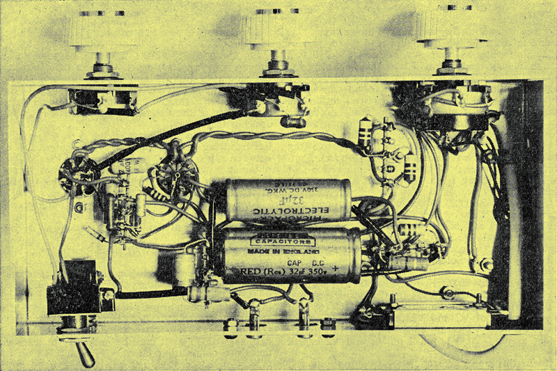
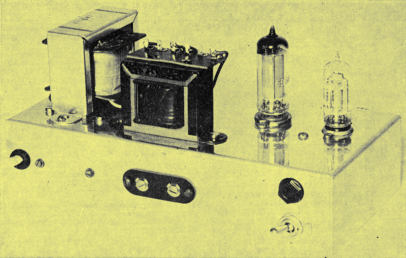
The layout under the chassis. Although compact, there is no crowding of components
Testing
The assembly of the amplifier is now complete and it has next to be tested. Two points have now to be mentioned so far as testing and subsequent use are concerned. First, the amplifier should not be operated without a speaker connected to it. This is because excessively high audio voltages may appear in the anode circuit of V2 if there is no load across the secondary of T1 and, if switch S1 happens to be open. Second, some form of supporting block should be used at the V1 end of the chassis if this is inverted on the bench. Without such a support the chassis will rest on the top of V2, with consequent risk of damage to this valve. The first step in testing is to visually check all wiring for poor joints, short-circuits between tags and any other obvious faults. Remove any excess blobs of solder which may have fallen into the chassis. If an ohmmeter is available check the resistance between the HT positive supply and chassis by connecting the meter between chassis and tags 10, 9 and 6 successively. The resistance should be well above 20 kΩ, the meter needle giving an initial kick due to the HT electrolytic capacitors charging.
The next task is to check whether the negative feedback is in correct phase. Connect a loudspeaker to the terminal board, close S1 and plug the amplifier supply lead into the mains. Switch on by means of VR3/S2, maintaining a grip on its control knob. If, as the valves achieve emitting temperature a howl or similar oscillation becomes audible from the speaker, switch off immediately. Reverse the connections at T2 secondary and switch on again. This time there should be no oscillation, indicating that the feedback is truly negative. When satisfied that the connections at T2 secondary tags are correct, they should be soldered up permanently.
The amplifier may now be checked finally with a suitable signal source such as a crystal pick-up. It should be found that all the controls work satisfactorily and that gain increases when S2 is opened. Some final operating points need to be dealt with. With S2 closed there should be, at worst, a very low hum level with no input and VR2 at maximum setting. Hum level in the prototype under these conditions was negligibly low. The tags of VR1 and VR2 are very prone to capacitive hum pick-up and care should be taken to keep mains wiring away from these circuit points. Some potentiometers on the home-constructor market have metal covers which are not, by reason of the potentiometer construction, automatically connected to chassis by way of the mounting bush. The use of such potentiometers for VR1 or VR2 may cause the appearance of hum. If a potentiometer of this type is employed for VR2, the metal cover may, if necessary, be earthed by connecting it via a short bare wire to the left hand tag (see the wiring diagram) of this component. If a similar potentiometer is used for VR1, earth its cover to the cover of VR2 by means of a short insulated wire.
Input signals must, of course, be applied by way of screened wire. Never attempt to obtain an input signal from an item of equipment whose chassis is connected to one side of the mains.
It should be remembered that the primary tags of the speaker transformer above the chassis are at HT positive potential. If there is a risk of these tags being touched when the amplifier is in use, the amplifier should be housed in a suitable cabinet. Ventilation is required at the rear of such a cabinet for the heat dissipated by V2 and the rear chassis apron area in contact with D1-D4.
It is recommended that a speaker of some 8 in. diameter be used with the amplifier, this being housed in a large cabinet to ensure a good bass response. Very small speakers should be avoided. Such speakers may even be damaged if the full output of the amplifier is fed to them.
The assembly and operating instructions are now concluded. The 'Neophyte' 5 Watt amplifier is complete and ready for use.
Components List
|