|
The Transistor: a three electrode germanium contact device
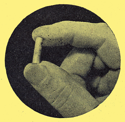
Indicating the size of a typical Transistor semi-conductor triode.
Working in Bell Telephone Laboratories, J Bardeen and W H Brattain have developed a three-electrode germanium crystal contact device, known as the Transistor, details of which have been published in the Physical Review, Vol. 74. July 15th, 1948. pp 230-233.
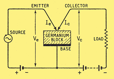
Basic circuit of the Transistor
Their experiments show, that by placing point contacts of tungsten or phosphor bronze in close proximity (0.05 to 0.25 mm) on the specially prepared surface of a germanium block, interdependence of currents in the vicinity of the contacts can be utilized to obtain power amplification of the order of 26 db.
A positive bias of about 1 Volt is applied to the 'emitter' contact, which also carries the input signal, and negative bias on the 'collector' contact is adjusted until the collector current is of the same order as the emitter. A large proportion of the emitter current passes to the collector, and amplification results from the fact that the collector contact, and the load to which it is matched, has an impedance about 100 times that of the input (emitter) circuit. Thus the input / output impedance relationships as well as the polarity of the 'HT' supply voltage are the reverse of those found in conventional thermionic triodes.
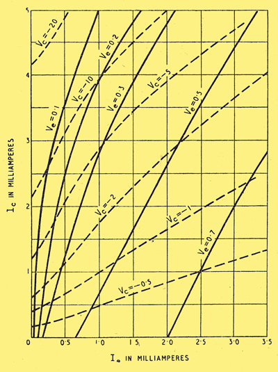
Typical DC characteristics. The currents are the independent variables and the corresponding voltages, the dependent variables.
Typical DC characteristics are shown above. The emitter current is given approximately by the expression:
Ie=f(Ve + Rf x Ic)
Where Rf is a constant which is independent of the bias. There is positive feedback, represented by the term Rf x Ic, which under some conditions may cause instability. The device can, in fact, be used as an oscillator.
Theory
A reasonable explanation of the a mechanism of conduction in the region of the contacts is possible in terms of statistical mechanics, but it is difficult to convey a plausible physical picture of the transport of current. According to prevailing theories, there are two types of semi-conductor, the n-type involving the migration of electrons and the p-type in which permissible but unoccupied electronic energy levels or 'holes' are propagated through the crystal lattice structure, and are equivalent to a flow of positive electricity in the opposite direction to the electron flow. The nature of the conduction is influenced by impurities in the material.
In the Transistor the main body of the germanium is of the n-type with a thin surface layer of p-type germanium. It is thought that the current between the emitter contact and the main body of the germanium, is conveyed by 'holes', and that a large proportion of these 'carriers' are attracted to the collector.
The mobility of the carriers is dependent on temperature and the field strength. In practice, the finite mobility is equivalent to transit time in a valve, and limits the response of the Transistor, at the contact spacing quoted, to frequencies below 10 MHz.
If satisfactory circuit techniques can be developed to meet the conditions of low input and high output impedance and positive feedback, and if signal/noise ratio is not unduly low, there would seem to be many applications in which Transistors could usefully take the place of valves.
Bell Telephone Laboratories have already constructed an experimental radio receiver with a power output of 25 mW, using Transistors throughout and have also demonstrated a repeater amplifier and an AF oscillator.
The DC power consumption is 0.1 watt, and the overall efficiency is 25 per cent.
|