|
Data on the Mullard E series - includes Short-Wave types.
The valves comprising the new range just introduced by Mullard and known as the 'E' series differ in several aspects from previous types. The outstanding feature is the use of a short cathode of high emission. This makes for a low heater current, good heat radiation, mechanical rigidity and a compact assembly. The cathode heating time is 10 seconds and all valves are designed for 6.3 Volts with the exception of the EK3, ECH2, and output pentodes, the valves take 0.2 A heater current, so that the power wasted in heating the cathode is only 1.26 Watts. Rectifiers, however, have 4 V filaments.
One factor which follows from the small dimensions of these valves is of particular interest to short-wave enthusiasts. Because of the closer electrode spacing the transit time of the electron is lower than in ordinary types and this results in a higher input resistance. The makers, in fact, claim that the performance of these valves at frequencies of the order of 56 MHz is intermediate between the existing series of English valves and the Acorn type.
Valves in this series are fitted with the side-contact base for which a smaller capacity is claimed than for the ordinary pin base; it is also specially designed to minimise RF losses between the contacts.
One of the most interesting of the new valves is the EF8, this is a low-noise RF pentode and as such it is of particular interest for short-wave work. Although the valve is called a pentode, it has actually four grids and so would more properly be termed a hexode. Unfortunately, this word is too much associated with the frequency-changer to render its use desirable for an RF valve.
The anode current of a valve is not uniform, but fluctuates, giving rise to the well-known valve hiss. In a RF stage the fluctuating component of the anode current is proportional to the square root of the anode current, the square root of the bandwidth and to a factor F which is dependent on the construction of the valve. It is convenient to express the valve noise in terms of an equivalent resistance Re which if connected in the grid circuit will produce the same noise through thermal agitation. The convenience is brought about by the ease with which it is possible to compare valve and circuit noise.
Expressed in this way Re = 2,000F2ia/g2 for a temperature of 300° and with ia representing the DC anode current in mA and g the mutual conductance in mA/V. The value of the valve as an amplifier increases with the mutual conductance, and if the anode current remains constant the equivalent noise resistance is inversely proportional to the square of this property. In general, however, anode current tends to rise with mutual conductance, and the valve with the highest value of g does not necessarily give the best signal-noise ratio. In general, anode current and mutual conductance are fixed by the other desired valve characteristics, and then the noise can be controlled only by the factor F. In the case of a saturated diode F is equal to 1, for there is then no space charge. In normal operation valves have some space charge and in the case of a triode F2 has a value of about 0.05 and considerably reduces noise. With a pentode, however, F2 is about 0.3; that is, for the same current the noise is about six times as great as with a triode.
Reducing Valve Hiss
There is thus scope for considerable improvement in the pentode, and it is found that with this type of valve F2 is roughly proportional to the ratio of the screen-grid current to the total cathode current. It is, therefore, essential to make the screen-current as low as possible. This can easily be done by reducing the number of turns on the screen-grid while keeping the wire diameter the same. Unfortunately, however, this has the effect of reducing the screening effect and the control grid-anode capacity increases.
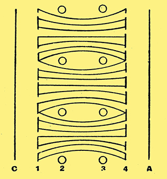
Fig. 1. This drawing shows part of the electrode assembly of the EF8; a low screen current is obtained by a beam-formation of the electron stream which is produced by the auxiliary grid G2.
In the EF8 the difficulty is overcome by adopting the principles of electron optics. An additional grid is mounted between the control and screen grids, and its turns are wound exactly in front of those of the screen. This grid is maintained at cathode potential. Consequently, the electrons passing this auxiliary grid are grouped in the form of a beam and pass through the interstices of the screen, comparatively few of them reaching the screen itself. The action will be clear from Fig. 1, which shows a sketch of part of the electrode system of the EF8. The cathode and anode are represented by the lines C and A respectively, and the control and suppressor grids by the dash-lines 1 and 4. The circles 3 represent the turns of the screen-grid and the circles 2 the turns of the auxiliary grid; the paths of the electrons are shown by the horizontal curved lines.
As a result of this construction the screen current of the EF8 is only 0.2 mA as compared with 4.25 mA. for the older VP4B. The factor F2 is only 0.084, giving an equivalent noise resistance Re of 4,100 Ω the noise level of the valve is thus of the same order as that of a triode. The resulting improvement is likely to be more noticeable on the short waves than the medium or long wave bands, for on the latter it is not usually difficult to arrange matters so that valve noise is negligible in comparison with circuit noise, but on short waves this is generally impossible. The low input and output capacities - 4.9 pF and 7.8 pF - are also helpful. The method of reducing the screen current which has been adopted has one disadvantage. To obtain an adequate electron flow, the auxiliary grid must have a fairly wide mesh and as the turns of the screen grid must correspond with those of the auxiliary grid the screen grid must also be of wide mesh. As a result the effective control-grid-anode capacity is increased. In the EF8 it is about 0.006 pF as compared with 0.0023 pF for the VP4B. The anode AC resistance, is also somewhat lower than usual, being about 0.5 MΩ.
The valve has a mutual conductance of 1.8 mA/ V, and in normal operation anode and screen supplies of 250 Volts are used, the auxiliary grid and suppressor are tied to the cathode and the grid has -2.5 Volts bias. The anode current is 8 mA and the cathode bias resistance should be 300 Ω.
Not only RF pentodes but frequency-changes have received considerable attention in this series of valves. It is well known that the octode suffers from two main disadvantages the oscillator frequency is liable to vary with a change in the control grid bias and there are coupling effects between the control and oscillator grids. These difficulties have been very largely overcome in the EK3 - the former by electron optical methods and the latter by neutralisation. In order to avoid frequency drift the current to grid 2 (oscillator anode) must not vary during the application of a control voltage to grid 4 (control grid) and the return of electrons from the virtual cathode in front of grid 4, to the oscillator space must be prevented.
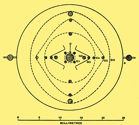
Fig. 2. The electrodes of the octode frequency-changer EK3 are illustrated in this diagram.
These results are obtained in the EK3 by the electrode structure-shown in Fig. 2. An electron beam passes through each of the four pins supporting grid 1 and through the openings in grid 3 into the outer part of the valve. There are thus four beams traversing grid 1. Grid 3 has two gaps and is enclosed by grid 4, the supporting pins of which face the exact centre of each of these gaps. These pins divide and deflect each beam into two halves, and as a result none of the electrons repelled from grid 4 can return through the gaps in grid 3 into the oscillator section.
As a result the mutual conductance between grids 4 and 2 becomes zero instead of 0.5 mA/V as in the case of the FC4 and EK2. Furthermore, the space charges between the cathode and grid 1 and between grids 1 and 2 are not affected by changes in the bias of grid 4, and these also have no effect on the mutual conductance between grids 1 and 2.
The first improvement results in the elimination of certain unwanted effects between the input and oscillator circuits which sometimes give rise to oscillation. The other two factors result in the virtual elimination of frequency drift.
In addition to the foregoing, the 'induction' effect has been largely eliminated in the EK3. This effect can be represented on the medium and long wavebands by a negative capacity between grids 1 and 4, and can be largely neutralised by the connection of an external capacity between these electrodes. On short waves, however, it can be demonstrated experimentally that complete neutralisation of the effect is impossible with only a capacitor.
The reason for this is the finite transit time of the electrons between grids 1 and 4, In the FC4 this time is 2 × 10⁻⁹ second, and at 15 metres this means a phase shift of some 14.5°. The effect can then be represented by a capacity and resistance in series between these two grids. Neutralisation can be effected by a similar external circuit and provided that the transit time is reasonably low this neutralisation will be independent of wavelength. In the EK3 this neutralising circuit is built into the valve and consists of a capacity of 1.6 pF in series with a resistance of 1,200 Ω.
Proper neutralisation, however, is obtained only for a particular amplitude of oscillator voltage on grid 1 - about 8-9 Volts. As this voltage usually varies somewhat over the tuning range, it should be adjusted to the optimum value at the highest frequency end of the band. An oscillator grid leak of 50 kΩ is recommended, and the optimum heterodyne is obtained when the current through it is 320 μA.
In order to keep frequency drift at a minimum it is essential that the screen voltage (G3, G5) be kept constant. The screen-feed potentiometer should consequently draw a heavy current; there is naturally a limit to the current that can be conveniently wasted in this potentiometer, but it must be remembered that frequency drift diminishes as the current increases.
As the complete elimination of the effect is impossible, it is important to choose an oscillator circuit giving maximum stability. The tuned anode circuit has much to commend it and gives a considerable improvement if the reaction coupling is not too tight. Owing to the high mutual conductance of the oscillator section of the valve - 4.5 mA/V - tight coupling is unnecessary.
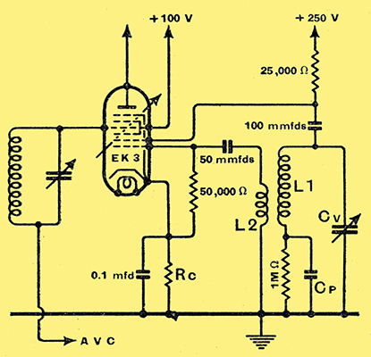
Fig. 3. The recommended circuit for the EK3 is shown here. A tuned anode oscillator is used.
The recommended circuit is shown in Fig. 3 and shunt feed of the oscillator circuit is adopted to avoid applying the HT to the tuning capacitor. One disadvantage is that the tuned circuit is damped by the 25 kΩ feed resistance, but this is not usually serious enough to cause any difficulty. Using this circuit but with a series resistance screen feed instead of the recommended potentiometer, the measured frequency drift at 15 metres for a control grid bias change of -2 to -20 Volts is claimed to be 4.5 kHz.
The valve heater consumes 0.72 A and it is rated for operation at 250 Volts for the anode and 100 Volts for screen and oscillator anode. The normal grid bias is -2.5 Volts. The conversion conductance is 0.65 mA/V with an AC resistance of 2 MΩ. Under operating conditions the oscillator anodes current is 6 mA., the screen current 5.5 mA., and the anode current, 2.5 mA. The input and output capacities are 14.5 pF and 15 pF. This, is not the only octode in the E series, for there is also the EK2. This is of more conventional design and has input and output capacities of 8.8 pF and 10 pF with a conversion conductance of 0.55 mA/V. The screen potential should be 50 Volts with 200 Volts for the oscillator anode.
Probably of more general interest, especially for short waves is the triode-hexode ECH2. This has characteristics similar to those of the TH4A in the 4 Volt range. Its heater consumes 0.95 A, and its input and output capacities are 8.0 pF and 13.0 pF. It has a conversion conductance of 0.75 rnA/V and an AC resistance of 1.5 MΩ.
Although the low-noise RF pentode in the E series is of special interest its advantages are largely confined to the first stage of amplification, and its low noise properties confer little benefit in later stages. Here other factors may be more important, particularly the variable-μ characteristics. As a result the range includes other types of RF pentode.
A variable-mu valve should have as low an anode current and as high a mutual conductance as possible at minimum bias, and the maximum bias needed for control should be as small as possible. Since the characteristics of a variable-mu valve are necessarily curved, there are several possibilities of trouble; there may be distortion of the modulated waveform, cross-modulation, modulation hum, and the introduction of harmonics of the carrier. This last is important in the IF stages of a super-heterodyne.
These troubles are minimised by the adoption of a valve characteristic of exponential form, having a flat slope when plotted on a logarithmic scale. Such a curve, however, leads to a low maximum value of mutual conductance or else a high anode current. For instance, for a mutual conductance of 2.0 mA/V and a maximum grid bias of -60 Volts, the anode current would be of the order of 14 mA.
In the case of the EF9, therefore, the desired characteristic is not a property of the valve alone, but of the valve in conjunction with the circuit. The desired result is secured by feeding the screen-grid through a voltage-dropping resistance instead of from the more usual potentiometer. The result is that as the grid bias is increased, the screen voltage rises.
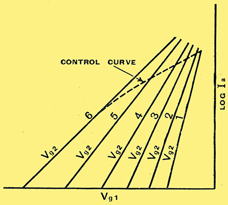
Fig. 4. When a screen voltage dropping resistance is used with a variable-mu valve, the effective control curve takes the form shown by the dash line.
Referring to Fig. 4, the solid line curves show the variation of anode current with bias for a series of values of screen voltage. With a constant-screen voltage the working point would be on the curve corresponding to the voltage selected. The dotted curve shows the effect of using a series resistance in the screen circuit. As the bias is changed the anode current alters according to this curve, but the characteristic for AC voltages is the solid line curve which intersects the working point.
The EF9 has input and output capacities of 5 pF and 7 pF with a grid-anode capacity of less than 0.003 pF. With 250 Volts HT supply, the screen should be fed through a 90 kΩ resistance, and the anode and screen currents respectively are 6.0 mA. and 1.7 mA. The mutual conductance is 2.2 mA/V at -2.5 Volts grid bias, and the AC resistance is 1.25 MΩ. The maximum grid bias is about 40 Volts.
The Duo-Diode
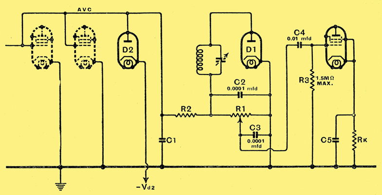
Fig. 5. This circuit shows how delayed AVC, detection, and noise suppression can be obtained with a duo-diode.
The range includes a duo-diode triode, the EBC3, but perhaps the EB4 duo-diode with separate cathodes is of greater interest in view of the wide variety of uses to which it may be put. Apart from AFC circuits, it finds application in noise suppression arrangements, and one circuit is shown in Fig. 5. This is an extremely simple arrangement, and to clarify the diagram the diodes are shown separately. One diode is used as a detector and fed from the IF amplifier in the usual way, the load resistance and by-pass capacitor being R1 and C2. The AF volts across this resistance are fed through the RC circuit C4 and R3 to the AF amplifier.
The cathodes of the controlled values are returned to the earth line and the grid circuits are returned through the usual filter C2 R2 to the diode load. The second diode, however, has its anode connected to the AVC line and its cathode taken to a point about 2 Volts negative with respect to earth.
In the absence of a signal D2 conducts and there is a current through R1 and R2 and this diode. The voltage drop across the diode is small compared with that across R1 and R2, and nearly the full 2 Volts is applied through the diode to the grids of the controlled valves for their initial negative grid bias. A fraction of this voltage equal to R1/(R1+R2) is applied to the anode of the detector diode D1. This diode is consequently non-conductive and inoperative, so that it does not respond to weak signals and gives noise suppression. When a strong enough signal is tuned in, however, D1 begins to operate as at detector in spite of the small negative bias on its anode; a current consequently flows through R1 and a potential is developed across this resistance, making the diode anode negative with respect to the cathode. When this potential exceeds 2 Volts the anode of D2 becomes negative with respect to its own cathode, and hence this diode becomes non-conductive. The initial bias is then removed from the controlled stages and the detector diode, for it has been overcome by the AVC voltage. For signal strengths great enough to produce more than about 2 Volts AVC bias, the operation of the circuit is identical with that of the ordinary simple AVC system, for D2 then plays no part. For weaker signals D2 introduces muting and a small delay on AVC.
The Triple Diode
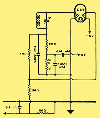
Fig. 6. The recommended detector and AVC circuit for the EB4 is shown here.
This circuit has the practical disadvantage that the delay voltage is equal to the initial. bias of the controlled valves. Consequently, if a large delay is heeded, the sensitivity is greatly reduced. This can be overcome by applying only a portion of the voltage across C1 to the controlled valves. If this is done, however, the AVC voltage is divided in the same ratio and the AVC characteristics suffer. Some compromise in design is thus needed. The recommended arrangement is shown in Fig. 6.
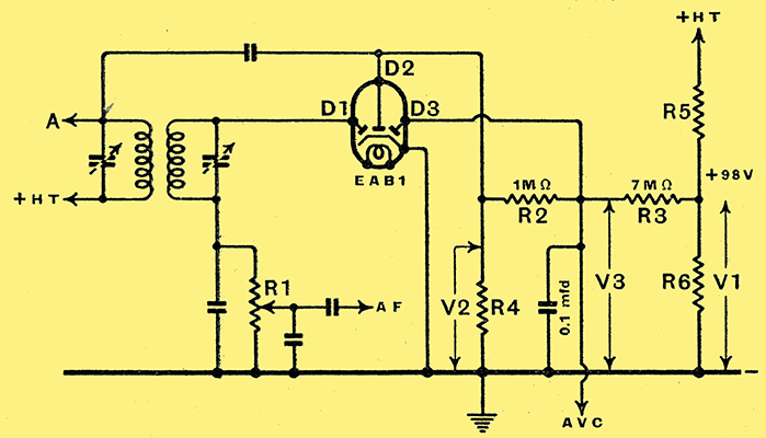
Fig. 7. The use of a triple-diode for detection and distortion-less deIayed AVG can be seen from this diagram.
Another of the new valves is also designed for use in AVC circuits; it is a triple-diode and is used in the circuit of Fig. 7. In the EAB1, one section D1 functions as a detector in the usual way and has the load resistance R1. The second section D2 is fed from the primary of the IF transformer; it has the-load resistance R4, and also functions as a detector without delay. Its output is used for AVC purposes, and delay is subsequently introduced by the third diode D3. This is done in order to avoid the distortion which would be caused by using a delay voltage on D2.
The resistances R5 and R6 form a potentiometer across the HT supply, and a voltage V1, which is positive with respect to the earth line, is applied to the delay circuit through R3. This makes the anode of D3 positive, and it then has a very low internal resistance. The AVC line is then very close to the potential of the earth line. When signal strength increases a voltage V2 appears across R4, making the anode of D2 negative with respect to earth. When V2 is great enough it overcomes the positive voltage on D3 and this diode becomes non-conductive and negative with respect to earth. The potential of the AVC line then follows it.
The voltage V3 on the AVC line is given by V3 = (V1R2 + V2R3)/(R1 + R2). In design V3 is taken as the voltage at which the delay action is just overcome and is about -0.8 Volt. V2 is then approximately equal to the peak RF carrier volts at which it is desired that AVC should begin to work. If this is 15 volts peak, then we have -0.8 = (V1R2 -15R3)/(R2 + R3), and the values assigned to the parts must satisfy this relationship. Suitable values in this case are V1 = 98 Volts, R2 = 1 MΩ, and R3 7 MΩ. Then after the start of AVC, V3 = 12.3 - 0.875 V2.
In addition to these special valves, the E series includes two output pentodes - the EL3 and EL6 - and a duo diode output pentode, type EBL1. This last is substantially the same as the EL3 with the additional diode elements.
The EL3 consumes 1.2 A. heater current and takes 36 mA anode and 4.5 mA screen currents at 250 Volts. The normal bias is -6 Volts and the mutual conductance 9 mA/V. The rated output is 4.5 Watts into a 7,000 Ω load. The EL6 is a larger valve, taking 72 mA. anode and 8.5 mA. screen currents and rated for 8.2 Watts output into 3,500 Ω. A pair in push-pull will deliver 16 watts for a no-signal anode current of 90 mA at full output this rises to 108 mA.
A cathode-ray type tuning indicator, EM3, is included in the range, and there are two rectifiers-_the AZ2 and AZ3 taking 2 A at 4 Volts. The AZ2 is directly heated and rated for 500-0-500 Volts at 120 mA. or 300-0-300 Volts at 160 mA, While the AZ3 is indirectly heated with a rating of 350-0-350 Volts at 120 mA.
|